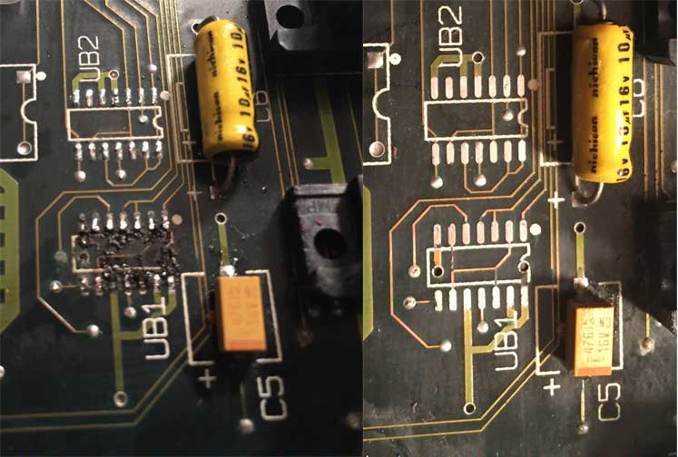
I recently repaired a Macintosh IIx I bought on eBay. It wouldn’t power on at all–both the rear power button and the keyboard power button did nothing. I was already aware that this system needs fresh batteries in order to boot, and I had removed the old batteries and replaced them with new ones, which didn’t make a difference. The real culprit: all of the surface-mount aluminum electrolytic capacitors had leaked electrolyte all over the logic board. This is a very common problem in older computers. These capacitors have a nasty habit of leaking after about 20 years or so. The electrolyte ate away at traces and several traces near capacitors were broken. Several IC pins were corroded really bad as well and had lost contact to their solder pads.
It was quite a journey figuring out how to fix it. The power button didn’t do anything, so I didn’t have a clue where to look. Luckily, an important figure in the Classic Mac community, Gamba, created a schematic of the power circuit. Sadly, Gamba passed away, but his site is still operational (update 4/5/2019: his site was finally taken down, but I updated the links to point to archive.org). I think there is a small error in his schematic, so I went ahead and fixed it. The fixed schematic is depicted below. The only change is the positioning of J18-15 and TS1 on the right side:
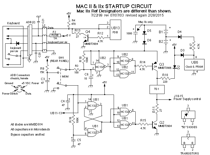
I began looking at this schematic and realized I didn’t have a clue what was going on in any of it. All of those NAND gates, diodes, and transistors looked intimidating. I buckled down and did my best to read the schematic and figure out what every piece does. After lots of experimentation and research, I feel like I understand this circuit pretty well now. I’ve decided to write this post to help explain the circuit and maybe help people in the future who are trying to figure out why their II/IIx won’t start up. Note: I am not an electronics expert. I’m trying my best, but I could be wrong about some details. Corrections would be appreciated!
Note that the diagram’s component numbering is for the Mac II. The IIx is slightly different. I would provide more detail, except my IIx logic board is a prerelease one that has the same component numbering as the II. So my IIx’s logic board’s component numbering matched this diagram. Other IIx systems do not match. [Update 6/28/2025: David Cook on the 68kMLA forums has discovered that earlier Mac II motherboards have a slightly different setup with the power off portion of the circuit, so be sure to check his post out for more details on that].
Let’s get started!
Overview
Here’s a broad overview of the different pieces of the circuit:
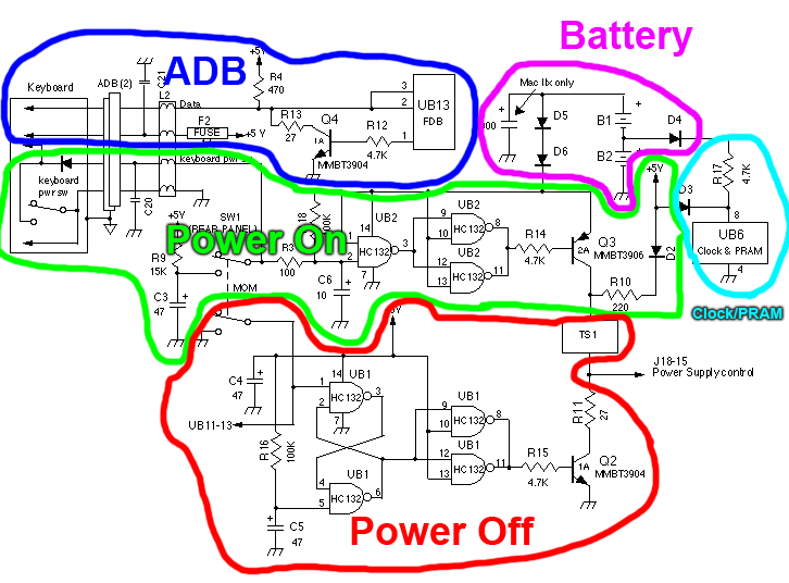
The ADB portion of this circuit is unrelated to this discussion, so I will skip it. Don’t worry–I have included the keyboard power button as part of my description of the power on circuit.
When I first looked at this diagram, for some reason I thought the top half was for the keyboard and the bottom half was for the rear power button. I was totally wrong. The keyboard and rear power button share most of the same power on circuitry. Now, I’m going to cover each section in more detail.
Batteries
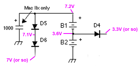
The two batteries B1 and B2 (3.6V 1/2 AA lithium) are in series with each other. This means they combine together to create a 7.2V voltage across ground and the positive terminal of B1. [Edit: Lee Carter pointed out in the comments below that the original batteries are actually 3V 1/2 AA, so they would actually total together to be 6V. You can correct the voltage numbers in the pictures and description below based on this new information] The three diodes seem to serve two purposes:
- Drop the voltage a little bit
- Protect against reverse polarity (putting the batteries in backwards)
In particular, D5 and D6 take the 7.2V voltage from the batteries and drop it down to about 7V or so. Normally these diodes would have a higher voltage drop, but you will see that while sitting idle, there isn’t much current being drawn from them, so the diode voltage drop is pretty low. D4 drops the 3.6V voltage a little bit, but I think its main purpose is to protect against reverse polarity. If you put B1 and B2 in backwards, D4 and D5 will prevent negative voltages from making their way to any other part of the logic board.
The 1000 μF capacitor is (I believe) the capacitor on the battery replacement board, and it can be found on both the II and the IIx, despite what Gamba’s diagram says. These computers originally came with the two batteries soldered directly to the logic board. When they needed to be replaced, there was a little circuit board that a service provider would solder on to replace the original batteries. It had two battery holders and a 1000 μF capacitor. I don’t fully understand the purpose of the capacitor, but it might be to make life easier on the batteries when the power button is pressed.
So this portion of the circuit takes two batteries as input, and as output provides a 3.3V-ish voltage rail and a 7V-ish voltage rail. I say “-ish” because I measured anywhere from 6.8V to 7V when I was debugging this circuit. But it’s somewhere in that ballpark. The 3.3V voltage is for powering the PRAM and clock while the computer is turned off. The 7V voltage is for turning the power supply on when you press either of the computer’s power buttons.
If you’re troubleshooting this portion of the circuit, make sure the cathode of D6 has 7V or so, and the cathode of D4 has 3.3V or so. If not, there’s something wrong with some of the traces and/or components pictured above. Check continuity between everything in the diagram above, and if needed, test D4, D5, and D6.
Clock/PRAM
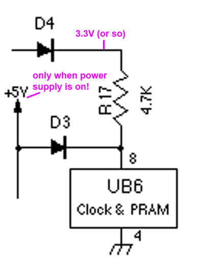
This portion of the circuit is responsible for powering the clock and PRAM. On most (all?) of the Macs that came after the II/IIx, this is the *only* thing the single 3.6V battery is used for, at least as far as I know.
Recall that I already explained that there is about 3.3V on the cathode of D4 coming from battery B2. The 4.7KΩ resistor R17 is limiting the amount of current that will be supplied to UB6, the clock/PRAM chip. So…when the computer is turned off, the battery B2 is powering UB6. D3 is preventing the battery voltage from going into the +5V rail (which will be 0V when the power supply is turned off).
When the power supply turns on, the +5V rail actually has 5V on it. D3 will allow the 5V to go through into UB6, so the +5V rail will power UB6. I believe the 4.7KΩ resistor (R17) makes it so that the 5V rail does most of the work powering UB6 instead of the battery when the power is on. D4 is also (I believe) preventing the circuit from sending +5V into the battery circuit when the computer is powered on.
This part of the circuit is pretty simple! I don’t think a problem in here would necessarily prevent the computer from turning on, but it might prevent settings from being remembered while the power is off.
Power On
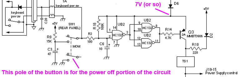
OK, here is where things really get interesting and more complicated. This is also where it will become obvious that both batteries must be installed in order for the II/IIx to boot. Recall that the cathode of D6 has about 7V on it or so. It powers UB2 (which is a 74HC132 containing four NAND gates–three are used, one is unused). UB2 doesn’t draw much current, so that’s why the diodes mentioned in the battery portion of the circuit don’t have much of a voltage drop. Without the batteries, these NAND gates will not be powered at all, and therefore the power circuit won’t work. It’s a good thing UB2 doesn’t draw much current, because otherwise the batteries would run out of juice too quickly.
Supplying 7V to the 74HC132 is a bit risky — it’s within the allowed range, but the datasheet I have recommends a maximum of 6V. Whatever–it seems to work. [Edit: The discussion about 3V vs. 3.6V above probably explains this discrepancy]
The 7V rail also goes to the emitter of transistor Q3, which is a PNP transistor. We’ll see in a minute, but when the power button is not being pressed, the transistor is turned off, so it shouldn’t be drawing any current.
Additionally, the 7V rail is directly connected to one of the inputs on each of the three NAND gates. In effect, it means each one of these NAND gates is really acting as an inverter (e.g. a logic 0 at the other input becomes a logic 1 at the output, and a logic 1 becomes a logic 0). This is because:
- 1 NAND 1 = 0
- 0 NAND 1 = 1
I’ll go into this in a bit more detail when I describe what happens when you press the power button.
Finally, the 7V rail goes through the 100KΩ resistor R18 to the second input of the leftmost NAND gate. This is a pull-up resistor that keeps the second input of the NAND gate pulled up to a logic 1 by default. The 100Ω resistor R3 is also connected to this part of the circuit, but the other end of it is floating when both power buttons are not being pressed, so it doesn’t really affect the circuit until a power button gets pressed.
So in the default state when the system is plugged in but no power button has been pressed:
- The leftmost HC132 NAND gate has both inputs at 7V. This means its output will be 0V.
- The output of that first NAND gate is fed into the other two NAND gates.
- Each of those NAND gates has one input at 0V, and one input directly wired to 7V, so they are both outputting 7V.
- Since 7V is going into the left side of R14, there is no current between the emitter and base of the transistor. The transistor is turned off.
- Because the transistor is turned off, the power supply control pin (J18, pin 15) is left floating (remember, the +5V output is not supplying 5V yet, since the power supply is off).
- Thus, the power supply stays off.
When the keyboard power button is pressed, the left side of R3 is grounded. This pulls pin 2 of the HC132 NAND gate to ground through the 100Ω resistor R3. So:
- The leftmost HC132 NAND gate has one input at 0V, and one input directly wired to 7V.
- The output of that NAND gate is thus 7V, which is fed into the other two NAND gates.
- Each of these NAND gates has 7V going into both input pins, so they are both outputting 0V.
- Since 0V is going into the left side of R14, current is flowing from the emitter of the transistor to the base of the transistor. The transistor is turned on and allowing current to flow from the emitter to the collector.
- Because the transistor is turned on, the power supply control pin is driven to 7V or so (just assume that TS1 is a short circuit for now–it will be described in more detail in the power off circuit description)
- Thus, the power supply turns itself on.
As soon as the power supply turns itself on, it begins outputting 5V. 5V goes through D2 and R10, pulling the power supply control pin up to +5V (minus the diode drop) through the 220Ω resistor. As soon as you release the power button, this mechanism keeps the power supply control pin high. Otherwise, the power supply would immediately turn itself back off.
The rear power switch does essentially the same thing as the keyboard power switch. When you press it:
- It completes a circuit to allow the battery to begin charging up capacitor C3, which is discharged when this process begins.
- The left side of R3 starts at 0V and slowly starts raising up as C3 charges.
- Since C3 starts at 0V, the same steps are followed as when the keyboard power button was pressed, and the power supply turns on.
- After the power supply turns on, 5V is available through R9, so C3 will charge up to 5V.
- C3 charging up to 5V is an important detail. If the button is later used for turning the computer off, the rear power switch won’t try to turn on Q3 at the same time it tries to turn the power supply off. It also gives you some time to release the power button before the system tries to turn itself back on again.
Wow! I may try to add some more diagrams in the future to depict it a bit more clearly. It’s a lot to digest.
You may be wondering: what is the point of the three NAND gates? At first glance, all they are effectively doing is repeating the input value that came out of R3. The purpose seems to be to allow better current drive capability for controlling the transistor, and a clean output that ensures that the signal controlling Q3 is either on or off, and not somewhere in between as capacitors charge up.
The three NAND gates essentially combine to create a buffer with double the current drive capability of a single NAND gate’s output. As long as all of the NAND gate pins are connected together and the NAND gates are working, you can assume that a low value at pin 2 of UB2 will turn the transistor on, and a high value at pin 2 will turn the transistor off.
Power Off
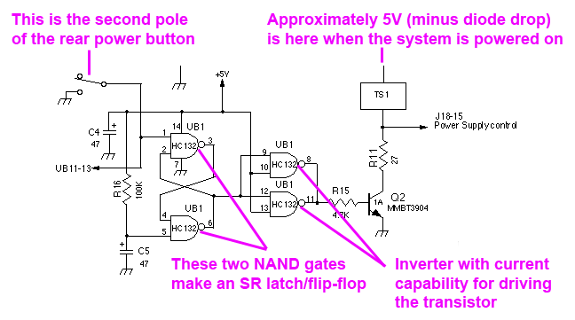
Just like the power on part of the circuit, the power off part of the circuit uses NAND gates that make it look way more complicated than it really is. These NAND gates are powered by the power supply’s +5V line. The two leftmost NAND gates form an SR latch. The SR latch’s top “set” input is connected to UB11, pin 13 (and the power button’s second pole). I believe this line is pulled up to +5V by a pull-up resistor inside the 6522 VIA (UB11), keeping it high (deasserted) while the computer is running. UB11 pin 13 is the /POWEROFF signal. At startup, C5 is fully discharged to 0 volts, so the SR latch’s “reset” input is low (asserted), which sets the SR latch’s stored “Q” value to 0. Then, C5 charges up, so the “reset” input goes high (deasserts itself) and stays deasserted while the computer is powered on. So the entire time the computer is running, the SR latch’s “Q” value is 0.
The !Q output of the SR latch is connected to the next two NAND gates, which act as an inverter just like in the power on circuit as I described earlier. So the output of the dual-NAND-gate inverter connected to R15 is really just the noninverted Q output of the SR latch, but with twice the maximum current. Thus, the voltage on the left side of R15 is 0V while the computer is on, keeping the NPN transistor Q2 turned off. Remember that the power supply control pin (J18, pin 15) is being pulled up to +5V in the power on circuit, keeping the power supply turned on.
Let me explain TS1 now. TS1 is a temperature switch. During normal operation, it acts like a short circuit. If the temperature gets too hot, it becomes an open circuit. If it becomes an open circuit, the power supply control pin is no longer pulled up to +5V, so the power supply shuts off (I’m pretty sure the power supply has a weak internal pulldown on that pin). During normal operation, TS1 will act like a wire.
When you tell the computer to shut down, the computer drives UB11 pin 13 (/POWEROFF) low. This causes the SR latch’s “set” input to go low, so it’s now asserted. This makes the !Q output low, which makes the inverter output high, so Q2 turns on, connecting R11 to ground. Now there is a 27Ω pulldown pulling the power supply control pin low, and a 220Ω pullup pulling the power supply control pin high (in the “power on” portion of the circuit). This is a voltage divider, so the voltage at the power supply control pin will be approximately 0.5V. This is low enough to tell the power supply to turn off.
If you press the power button on the back of the computer, the same thing happens — it connects the SR latch’s top “set” input to ground, and the exact same thing happens.
Troubleshooting
OK, so I have tried my best to explain what’s going on in each portion of the circuit. If you have a broken power circuit, how do you fix it?
The system will not power on
First of all, there are a few traces that have a tendency to go bad because they run nearby leaky capacitors:
- Make sure that the rear power button, R3, and the pin of L2 that goes to the keyboard power button are all connected together. (Note that R3 is on the bottom of the board)
- Make sure that R3, R18, C6, and pin 2 of UB2 are all connected together.
Of course, make sure you have removed, cleaned around, and replaced all of the electrolytic capacitors on the logic board.
Make sure that all of the connections between R3, UB2, R14, and Q3 are OK. If you can, use a voltmeter to verify that the NAND gates are operating as expected when you press either of the power buttons. You can do this with the logic board out of the computer as long as the batteries are installed.
Check the power supply control pin (J18, pin 15) to see if it’s correctly getting a voltage when you press either of the power buttons. If it is, there’s a chance that the power supply is at fault.
UB2 is somewhat near a capacitor. There’s a good chance that some of its pins have lost connectivity due to corrosion. Check every pin on UB2 and make sure it has connectivity as shown in the schematic.
The keyboard power button works, but the rear power button doesn’t
There are only a few parts of the circuit that could cause this. Make sure R9, C3, the rear power button, R3, and the keyboard power button pin of L2 are all connected as shown in the schematic diagram. For the rear power button to not work when the keyboard does, one of the connections between those components has to be broken.
The system powers on, but it won’t power off
UB1 is extremely close to a capacitor. There’s an extremely good chance that it has lost some connectivity due to corrosion. Verify all connections.
See if the output of UB1 pin 8/11 is correctly going high when you press the rear power button while the system is on. If not, follow the circuit and see where the broken trace is.
Final thoughts
I thought this would be a good idea to explain the circuit in more detail. This has turned into quite a long-winded explanation, and it doesn’t have quite as many pictures as I would have hoped. Maybe this would be better as a video or an animation that shows what the circuit is doing. For now, I hope this is enough to help someone out there troubleshoot their Macintosh II/IIx power circuit.
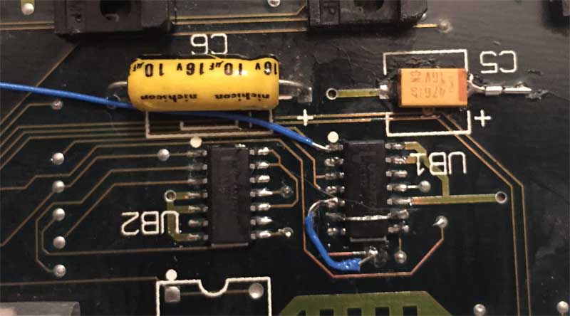
In my particular case, a trace was broken in the R3-R18-C6-UB2 group of pins that should be connected together, and UB1 was completely covered in capacitor leakage, which had very badly corroded its pins and solder pads. I ended up replacing both UB1 and UB2 to be safe. A trace between a via and C5’s positive end was also broken and needed a patch wire. I had to run several patch wires to repair broken traces:
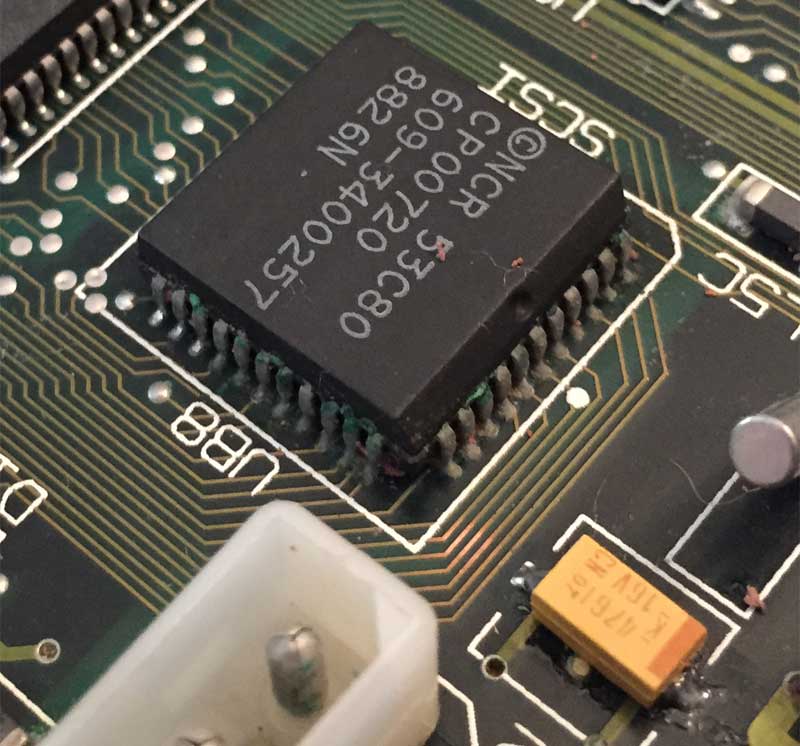
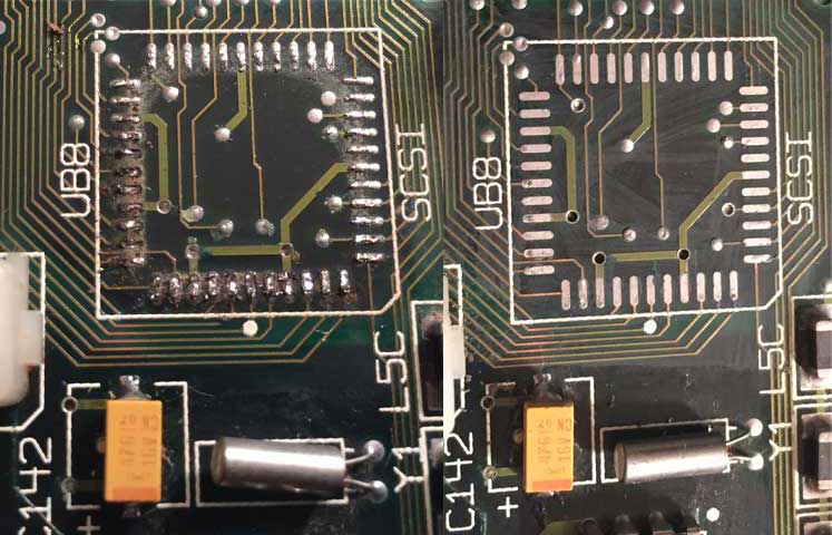
By the way, this wasn’t the only problem with my IIx. This was actually the last part of the logic board that I fixed. The whole power on circuit can be bypassed by tapping a 3.6V battery between ground and the power supply control pin, so I did that for testing until I repaired this circuit. The power supply would turn on, but nothing would happen. It turns out that there were a ton of other traces that were corroded. The 53C80 SCSI chip (again, near a capacitor) was very badly corroded, so I removed it, cleaned the solder pads, and replaced it with a new one. One of the solder pads had a break from its trace, so I had to run a patch wire. I also found several other broken traces on solder pads near two chips on the board.
It’s been a wild ride, but I now have a working IIx!


