It didn’t work. The screen was black, it played the startup sound, and then immediately followed up with the “Chimes of Death”. Nothing else happened from that point on. Here’s what it sounded like:
This was a little frustrating because last year I had already replaced all of the capacitors and cleaned where they had leaked, so I didn’t expect to encounter any problems with it so soon. The machine had worked fine the last time I’d tried it! But despite all that, something was failing during the power-on tests in Apple’s ROM, prompting it to play the chimes of death. I remembered that people have been working towards documenting the Mac ROM startup tests and using them to diagnose problems, so I decided to give it a shot and see if Apple’s Serial Test Manager could identify my Performa’s issue. Where was the fault on this complicated board? Sure, I could test a zillion traces by hand, but why bother when the computer already knows what is wrong?
The first update is that some extra discussion took place in the comments of my original post. Reader “Greg” pointed out that there was an Apple employee named John Yen who worked on the Mac OS during the System 7 era, and suggested he might be the “jy” in the associated “msjy” creator code. That would leave “ms” potentially being Microseeds, which is the company that developed Apple Backup.
This led me to search further, and I stumbled upon Apple’s patent for the automatic OS recovery functionality filed in 1994. It was granted in 2002 and expired in 2019. John Yen is listed as the inventor. The patent contains some screenshots of the exact UI that I experienced while testing the functionality. I never thought to look through patents, but I should have. They are definitely a useful tool for historical research on this type of stuff. I thought that was a really cool discovery. Thanks, Greg!
I was recently poking around inside the original Power Macintosh G3’s ROM and accidentally discovered an easter egg that nobody has documented until now.
This story starts with me on a lazy Sunday using Hex Fiend in conjunction with Eric Harmon’s Mac ROM template (ROM Fiend) to look through the resources stored in the Power Mac G3’s ROM. This ROM was used in the beige desktop, minitower, and all-in-one G3 models from 1997 through 1999.
As I write this post in mid-2025, I’m having a really difficult time accepting the fact that the Power Mac G3 is now over 27 years old. Wow!
While I was browsing through the ROM, two things caught my eye:
First, there was a resource of type HPOE which contained a JPEG image of a bunch of people, presumably people who worked on these Mac models.
This wasn’t anything new; Pierre Dandumont wrote about it back in 2014. However, in his post, he mentioned that he hadn’t figured out how to display this particular hidden image on the actual machine. Several older Macs have secret keypress combinations to show similar pictures, but the mechanism for displaying this one was a complete mystery.
As part of my research into the Macintosh Performa 550’s factory recovery partition, I paid a lot of attention to eBay listings for these computers. I came to an interesting discovery that I had already suspected: big CRT-based Macs in this form factor are regularly damaged in shipping after being sold on eBay.
Most vintage computer enthusiasts are well aware of this, but the plastic in old computers tends to become very brittle as it ages. With Macs in particular, machines made from 1993-ish onward seem to really be affected by this issue. I’ve seen this with my own eyes, too. The CD-ROM bezel on my Quadra 840av fell off because several very thin plastic clips snapped off. Good luck finding one that hasn’t already broken off. One of the clips that holds the top case in place on my Power Mac 6100 also broke off. And I, too, once received a Performa 550 that was destroyed in shipping.
For what it’s worth, I have experienced success with smaller “pizza box” Macs shipped to me. They are definitely from the same era of terrible plastic, but they have always been generously covered in all directions with bubble wrap and none of the ones I have received have ever been damaged in transit. I think the fact that they aren’t super heavy or large helps a lot.
I was curious about bigger, heavier machines though, especially since I had experienced destruction on one myself. I decided to do a quick little research project on eBay. I went through all past auctions I could find for the Macintosh Performa/LC 5xx form factor. Sadly, eBay’s history doesn’t go back very far, so it’s hard to get a decent sample size. Regardless of the lack of data, what I found doesn’t look promising for prospective buyers. Out of 12 total computers sold, I found:
In my last post about hard drives that go bad over time, I hinted at having rescued a lost piece of obscure Apple software history from an old 160 MB Conner hard drive that had its head stuck in the parked position. This post is going to be all about it. It’s the tale of a tad bit of an obsession, what felt like a hopeless search, and how persistence eventually paid off. There’s still an unsolved mystery too, so I’m hoping others will see this and help to fill in the blanks!
This whole saga starts with a very interesting blog post written by Pierre Dandumont in 2022. Pierre’s (excellent) blog is in French — Google does a good job of translating it for me. He found a quote in a book referring to special functionality bundled with Apple’s Macintosh Performa 550 computer:
The LC 550’s Secret Partition
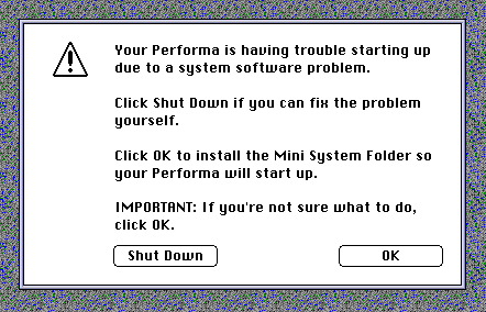
If Apple’s programmers, in creating the Performa series, were aiming to make idiot-proof computers, they were serious about it. The Performa 550 is an amazing case in point. When you run the included Apple Backup program (see Chapter 15), you get a little surprise that you didn’t count on: a hidden partition on your hard drive!
This invisible chunk of hard drive space contains a miniature, invisible System Folder. Apple’s internal memo explains it this way:
“When a system problem (one that prevents the Performa from booting) is detected, a [dialog box] informs the user of a system problem. The user can choose to fix the problem manually or to reinstall software from the backup partition’s Mini System Folder.”
If you choose to reinstall your System software, you get the wristwatch cursor for a moment while the miniature System Folder is silently copied to your main hard-drive partition. The Performa restarts from the restored hard drive, and the invisible system partition disappears once again.
We got a Performa team member to admit that this kind of sneaky save-the-users-from-themselves approach may well be adopted in other Performa models.
Who knows what goodness lurks in the hearts of men?
As part of my work toward an upcoming post about a lost piece of very obscure Mac history that has finally been found, I’ve been playing around with old Apple-branded SCSI hard drives made by Quantum and Conner in the 1990s. What I’m about to describe is already common knowledge in the vintage computing world, but I thought it would be fun to share my take on it anyway.
What I’m talking about is how a lot of these hard drives just refuse to work anymore. This is very common with old Quantum ProDrive models, like the LPS or the ELS. The drive spins up, you don’t hear the expected pattern of click sounds at startup, and then after a few seconds, it spins back down.
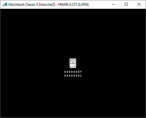
This is the story of how Apple made a mistake in the ROM of the Macintosh Classic II that probably should have prevented it from booting, but instead, miraculously, its Motorola MC68030 CPU accidentally prevented a crash and saved the day by executing an undefined instruction.
I’ve been playing around with MAME a lot lately. If you haven’t heard of MAME, it’s an emulator that is known best for its support of many arcade games. It’s so much more than that, though! It is also arguably the most complete emulator of 68000-based Mac models, thanks in large part to Arbee‘s incredible efforts. I will admit that I’ve used MAME to play a game or two of Teenage Mutant Ninja Turtles: Turtles in Time, but my main use for it is Mac emulation.
Here’s how this adventure begins. I had been fixing some issues in MAME with the command + power key combination that invokes the debugger, and decided to see if the keystroke also worked on the Classic II. Even though this Mac model has a physical interrupt button on the side, it also has an “Egret” 68HC05 microcontroller for handling the keyboard and mouse (among other things) that should be able to detect the keypress and signal a non-maskable interrupt to the main CPU. I believe the Egret disables this keystroke by default, but MacsBug contains code that sends the command to enable it.
I didn’t get very far while testing the command+power shortcut in MAME’s emulated Classic II, because I observed something very odd. It booted up totally fine in 24-bit addressing mode, but I could not get it to boot at all if I enabled 32-bit addressing, which I needed in order for MacsBug to load. It would just pop up a Sad Mac, complete with the Chimes of Death. On this machine, the death chime is a few notes from the Twilight Zone theme song.
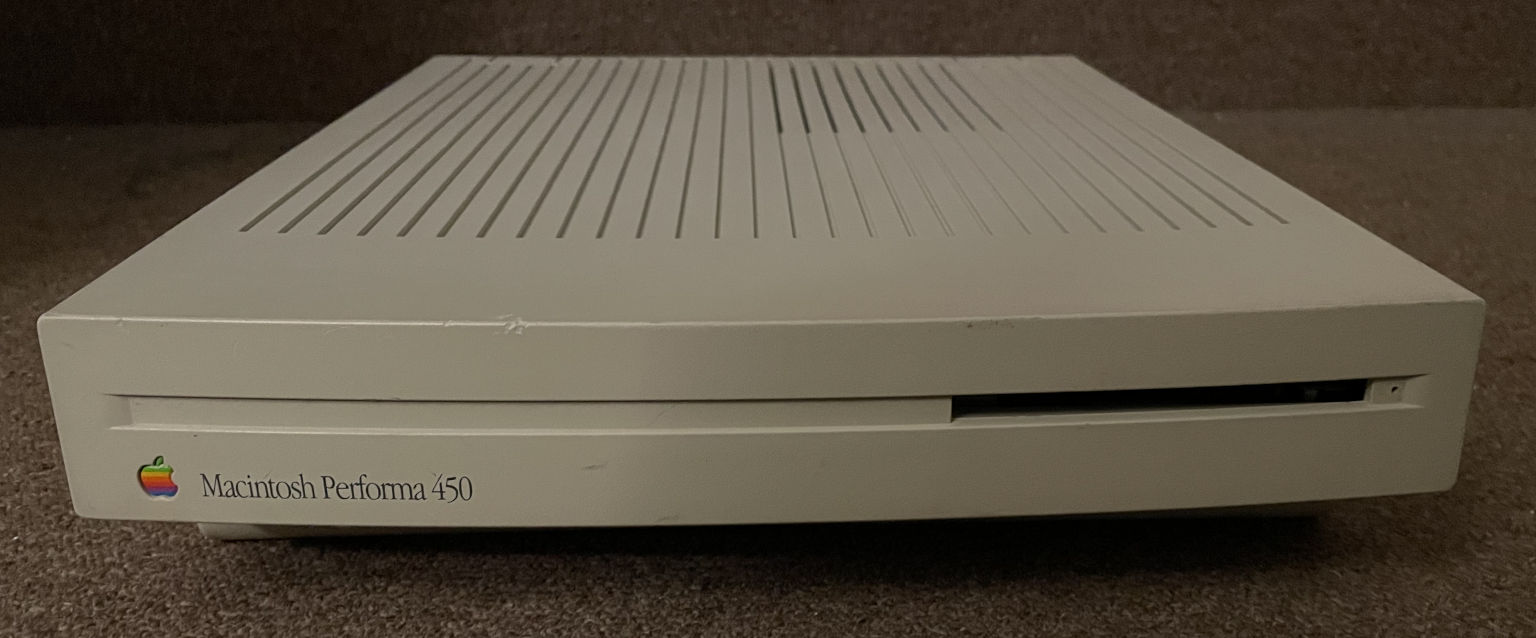
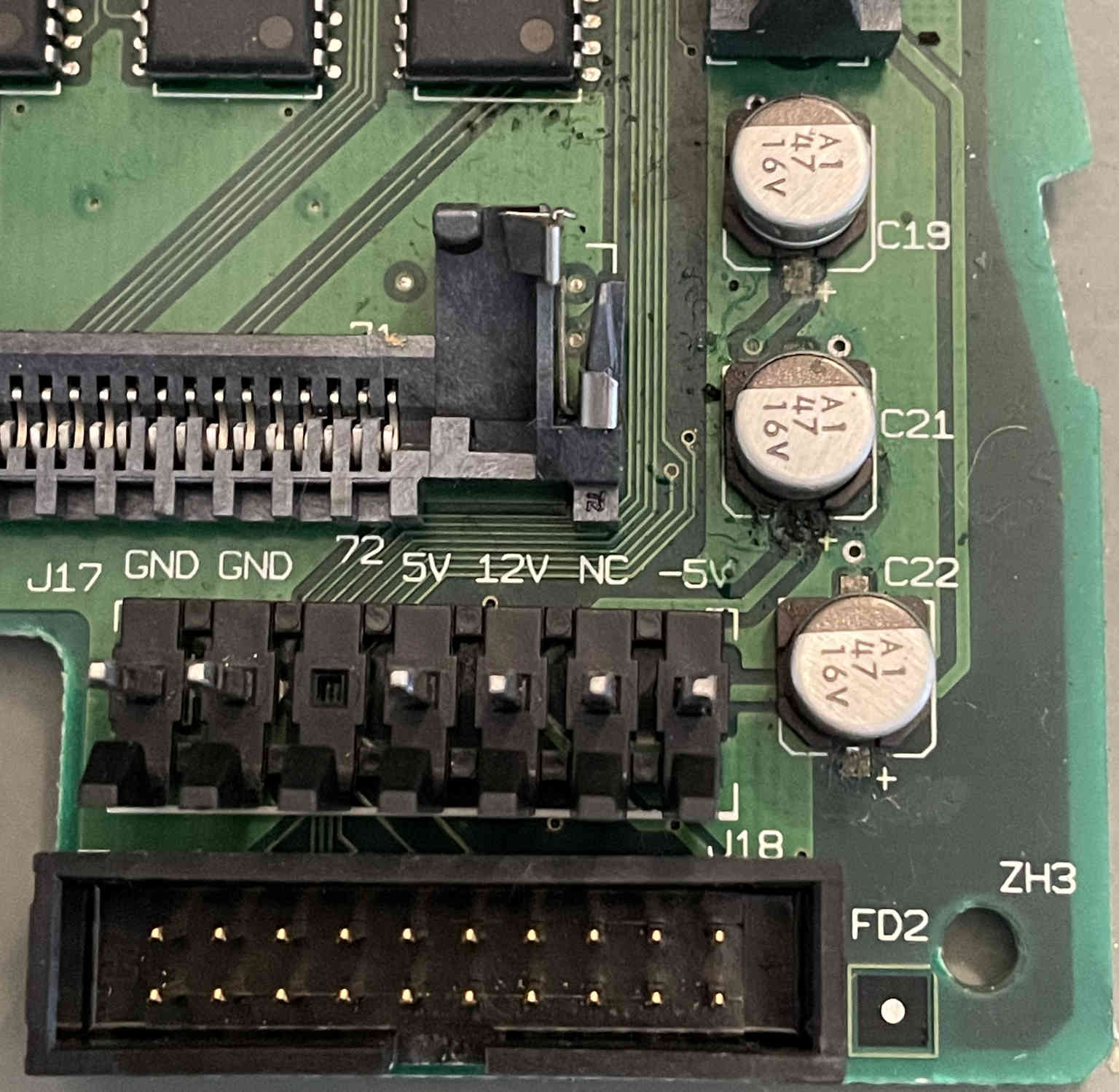
There have been some past rumblings on the internet about a capacitor being installed backwards in Apple’s Macintosh LC III. The LC III was a “pizza box” Mac model produced from early 1993 to early 1994, mainly targeted at the education market. It also manifested as various consumer Performa models: the 450, 460, 466, and 467. Clearly, Apple never initiated a huge recall of the LC III, so I think there is some skepticism in the community about this whole issue. Let’s look at the situation in more detail and understand the circuit. Did Apple actually make a mistake?
I participated in the discussion thread at the first link over a decade ago, but I never had a machine to look at with my own eyes until now. I recently bought a Performa 450 complete with its original leaky capacitors, and I have several other machines in the same form factor. Let’s check everything out!
Here’s the affected section of the board before I removed the original capacitors. You can see that all three of these caps (C19, C21, and C22) have their negative side pointing upward, matching the PCB silkscreen that has the + sign at the bottom.
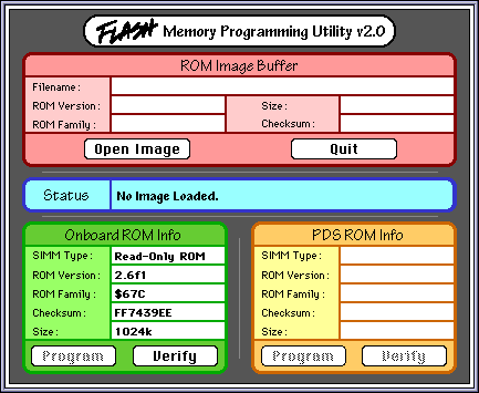
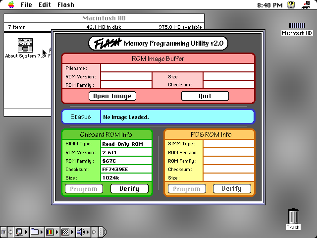
In my last post, I figured out how to use Apple’s leaked Flasher utility from the 1990s to reflash a ROM SIMM inside of my Performa 630. It’s basically the Mac equivalent of a BIOS update, but only for Apple’s developers. The research involved in that post was quite a journey of reverse engineering from both a software and hardware perspective. I had to disassemble the code to figure out which computers were compatible and what the software was expecting to find. I also had to create a replica of an Apple development ROM SIMM that was wired exactly the way Macs of the era expected it. Although I was very excited about my discoveries, one big question remained:
What was the purpose of the bottom right half of the main window labeled “PDS ROM Info”? And what would it take to enable it?
After I wrote about the possibility of programmable Mac ROM SIMMs in Quadras a couple of months ago, I suspected that there had been a way for developers at Apple in the 68k Mac era to reflash the ROM in their Macs during development, just like BIOS updates on PCs. The reason I believed this is because the ROM SIMM socket in the Quadras brought out pins for 12V (VPP) and write enable (/WE). I had verified that the write enable pin was going into the memory controller chip in several Mac models, so I was pretty confident that in-system programming was possible.
As luck would have it, multiple people pointed out to me that an Apple internal utility used for ROM flashing had been uploaded to the Macintosh Garden. It was recovered from a prototype PowerBook 520 purchased in 2020. Of course, I had to download this utility and figure out how it works.
I ran it on my LC 475 and this is what it looked like: