In my last post, I figured out how to use Apple’s leaked Flasher utility from the 1990s to reflash a ROM SIMM inside of my Performa 630. It’s basically the Mac equivalent of a BIOS update, but only for Apple’s developers. The research involved in that post was quite a journey of reverse engineering from both a software and hardware perspective. I had to disassemble the code to figure out which computers were compatible and what the software was expecting to find. I also had to create a replica of an Apple development ROM SIMM that was wired exactly the way Macs of the era expected it. Although I was very excited about my discoveries, one big question remained:
What was the purpose of the bottom right half of the main window labeled “PDS ROM Info”? And what would it take to enable it?
PDS stands for Processor Direct Slot. It’s an expansion slot that provides most of the CPU’s signals and can be used for adding things like Ethernet, a video card, or an accelerator. If you look at the comments on my last post, you will see some discussion about the PDS cards used by the Flasher app (thanks Al!). It sounds like they were used to flash programmable ROM SIMMs/DIMMs, and there were multiple generations of cards. That makes sense, because the list of compatible models covers a variety of systems with different PDS slots. Some of the Quadra machines like the 700, 900, 650, and 800 have a 140-pin 68040 PDS slot. The LC 475, 575, 580, and 630 have the 96-pin LC PDS slot that came from the original Mac LC, with an extra set of 18 pins that can optionally be used by fancier cards. The 610 has a card slot that takes an adapter board to give you either a NuBus slot or 140-pin PDS slot.
Even though I still have no idea what Apple’s original PDS cards used by developers looked like, I really wanted to rig something up to get the PDS portion of this software working. So I went to work disassembling the Flasher utility and researching classic Mac hardware and Motorola MC680x0 processors.
When I was first disassembling Flasher, I noticed a big table of compatible flash ROMs. A large portion of the entries were marked as PDS, which I wasn’t interested in at the time, so I had mostly ignored them. I spent a little more time investigating them this time around. All of the PDS entries use read and write addresses in the 0xExxxxxxx range, which corresponds with “slot E”. That makes total sense because that’s where Quadra PDS cards are expected to be mapped in memory. Looking through the entries, I found that the Lobos SIMM I replicated is also supported on the PDS side. The base read address is 0xE0000000, while writes use 0xEC000000. Other than that, the table entry seems to be pretty much the same as the entry used for an onboard SIMM of the same type. There are also a bunch of other table entries with additional options that would require further reverse engineering to fully understand. Let’s focus on just this one table entry.
I began to think: what would it take to create a PDS card with a 64-pin ROM SIMM socket so I could program my replica Lobos board through the PDS slot? All it would need to do is map the flash into memory at 0xE0000000 for reads and 0xEC000000 for writes. That doesn’t seem too complicated, right? I decided to jump in and figure it out.
I started by deciding which Mac I would use for this experiment. I opted for my LC 475.
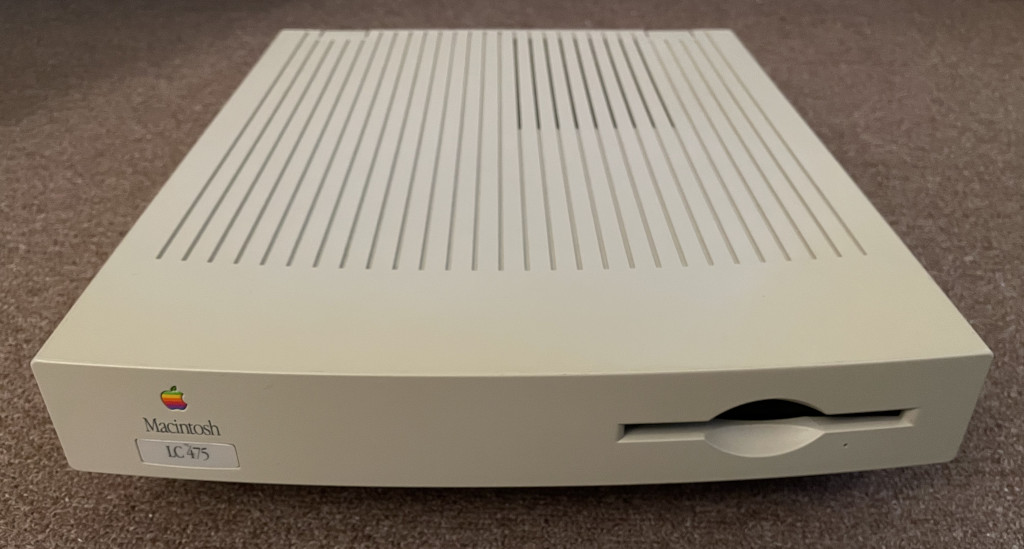
It has an LC PDS slot, which uses a readily available 96-pin Eurocard connector and as an added benefit is the simplest of all of them.
Even though the Quadras have 68040s, this slot pretty much pretends to be a 15.6672 MHz 68020 so that cards designed for the original Mac LC will still work. Simple is good! Also, the case is really easy to open up. My Performa 630 would be a poor choice for this experiment because you have to shove the logic board into the case in order to start it up.
I looked at sections 3 and 5 of the MC68020 user manual to get an idea of what kind of logic would need to be implemented by my PDS card. It was intimidating at first, but after spending some time thinking about it, I came to the conclusion that it really isn’t too complicated. Address strobe (/AS) goes low to indicate that a valid address is on the address bus. Data strobe (/DS) also goes low, either at the same time or shortly afterward depending on whether it’s a read or write cycle. The RW signal tells me whether it’s a read or a write.
That’s pretty much it in a nutshell! My PDS card’s job is to detect when an address I care about is being accessed, do the read or write requested, and then briefly drive /DSACK0 and /DSACK1 low to tell the CPU that I completed the operation and it was a 32-bit transfer. Obviously, the card has to do this in a way that follows all timing requirements as stated by the datasheet.
Programmable logic seems like the correct solution for this as opposed to a microcontroller. Either that or a bunch of logic gate ICs. I messed around on EDA Playground (a really cool site, by the way) to see what read and write cycles would look like and decide on a strategy to handle them. I made a Verilog testbench that performs a few read and write cycles based on the spec in the 68020 manual. Here’s an example of a read cycle to 0xE000000 assuming no wait states are needed:
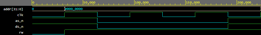
The read cycle begins with the rising edge of the clock. It puts the address onto the address bus and also signifies whether it’s a read or write. At the next falling edge, it asserts /AS and /DS. This is the signal to my PDS card to actually do something. At the final falling edge, it saves the data that has been presented on the data bus and deasserts /AS and /DS. Writes are similar, but /DS is asserted a cycle later instead.
I found that for both reads and writes, the easiest approach would be to assert /DSACK0 and /DSACK1 immediately as soon as /AS went low. Then I could deassert it when /AS went high again. I didn’t even need to look at /DS. I could use this exact same logic to assert the output enable (/OE) or write enable (/WE) signal on the flash chips too. Here’s what that would look like for a read cycle:
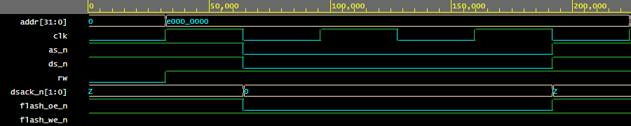
A write cycle would look very similar. The CPU will provide data to write on D[31:0] and will assert /DS slightly later than during read cycles. I would just need to pulse the /WE pin of the flash chips instead of /OE.
This arrangement provides plenty of time for the flash chips to do their thing. The /OE or /WE pulse width is about 127 nanoseconds, which is plenty. There is also plenty of setup and hold time on both the falling and rising edge of the /WE pulse for write cycles. The really nice thing about this design is it’s purely combinational logic. The rule is simply: whenever the address matches and /AS is asserted, assert /DSACK and either /OE or /WE, depending on the RW signal.
Determining if the address matches ended up being an interesting rabbit hole. Knowing that PDS cards are mapped to slot E, you might think you need to make sure that A[31:28] == 0xE or something like that. But no, the LC PDS slot is weird. The 96-pin portion of the connector common with earlier LC series Macs doesn’t even have A30 through A28 populated. It only has A31. Also, there’s a whole other 24-bit addressing mode to think about. Apple details this in the LC 475 developer note, with a sample circuit for generating a card select signal:
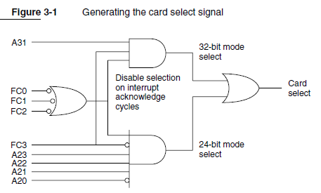
Looking at FC0 through FC2 is important so that you can differentiate between normal read cycles versus special CPU space cycles such as interrupt acknowledge cycles. FC3 tells you whether 24-bit addressing is enabled. In 24-bit mode, PDS accesses are recognized by A[23:20] equaling 0xE. In 32-bit mode, you just have to check if A31 is high. This all seemed a bit on the complicated side to me, but I was pretty sure I could ignore supporting 24-bit mode because I already knew that the Flasher utility puts the system into 32-bit mode behind the scenes when doing operations. After all, the table entry has a read address of 0xE0000000, which is not a valid address with 24-bit addressing.
It was around this time that I started looking at an LC PDS card that I have on hand: an Apple Ethernet LC Twisted-Pair card. I thought it would be a good opportunity to double check my work and see if my approach was sane, especially since it doesn’t have any special ASICs other than an Ethernet chipset.
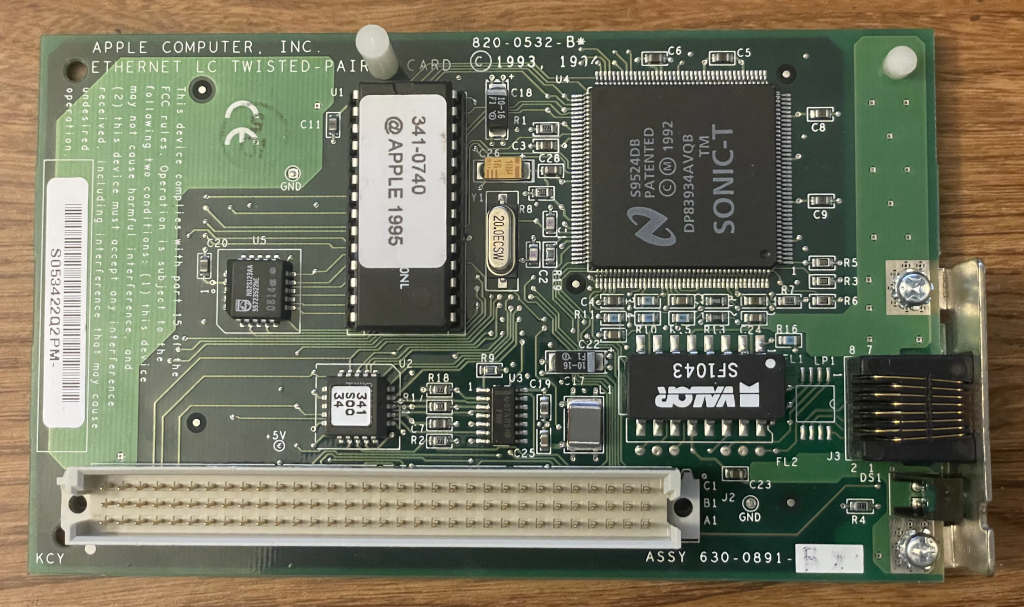
This card has a PROM chip of some kind (U1) that is clearly used as a declaration ROM for identifying itself to the system. This means that the card is going to have some glue logic for hooking up this PROM chip to the address and data buses, which is exactly what I needed to accomplish too. U2 seems to be some kind of PLD (a PAL16V8/GAL16V8 I think) which is definitely in control of /DSACK1 and the flash /OE pin, as well as other stuff like a chip select for the Ethernet chip. It’s looking at a handful of address lines, /AS, /FC3, and some other stuff that wasn’t immediately obvious.
One puzzling thing I found was that FC0-2 didn’t go anywhere on this card. I thought Apple said you needed to use them to make sure you didn’t accidentally treat interrupt acknowledge cycles as read cycles? Well…it turns out that there are other ways for detecting them that don’t require looking at FC0-2. I asked about it on 68kmla. ymk gave me some great advice: if you don’t need the full PDS address space, you can detect interrupt acknowledge cycles by looking at some of the address bits instead. Interrupt acknowledge cycles are guaranteed to have most of the address bits set to 1. This appears to be the approach Apple used on their Ethernet card. I experimentally determined that if A24 is high, the card doesn’t respond. I think it’s looking at this rather than FC0-2. It’s a lot simpler to implement if you don’t need the full address space. I decided to use Apple’s strategy on my card too.
Now I was ready to actually think about making this PDS card. I had an idea of what logic needed to be implemented, and I also was pretty confident about wiring. Just hook up all of the data and address lines from the ROM SIMM socket directly to the PDS slot, and then use a programmable logic device of some kind to handle bus control and flash write/read cycle control.
I had a decent idea of what the Verilog would look like for my glue logic. Something like this:
module flashcontroller(a31, a27, a24, rw, as_n, flash_oe_n, flash_we_n, dsack_n);
  input a31;
  input a27;
  input a24;
  input rw;
  input as_n;
  output flash_oe_n;
  output flash_we_n;
  output [1:0] dsack_n;

  wire pds_select = a31 & ~a24;

  assign flash_oe_n = ~(pds_select & rw & ~as_n);
  assign flash_we_n = ~(pds_select & ~rw & ~as_n & a27);
  assign dsack_n = pds_select & ~as_n ? 2'b00 : 2'bzz;
endmodule
A note on this: I’m looking at A27 because write cycles in the software are addressed to 0xECxxxxxx. I figured it would make sense to restrict valid write cycles the same way. I just silently ignore write cycles that don’t have A27 high. I could have also looked at A26, but I thought A27 by itself was sufficient.
I wasn’t sure exactly what type of programmable logic device to use for this. I probably could have found a fancy 5V CPLD, but I opted for something pretty simple that could be found in DIP form factor to make for easy prototyping. Microchip’s ATF22V10C seemed like a great candidate.
I quickly realized that Verilog would be useless for this particular task. Simple PLDs seem to be more typically programmed using an old language called CUPL. It wasn’t too crazy to learn. Microchip provides WinCUPL as a free download. It’s pretty old and buggy, but it gets the job done even in Windows 10. There are also open source alternatives such as galette.
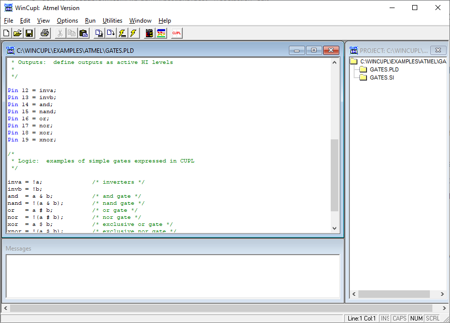
Here’s my equivalent logic in CUPL suitable for programming into the 22V10:
PIN 2 = A31;
PIN 3 = A27;
PIN 4 = A24;
PIN 5 = RW;
PIN 6 = !AS;

PIN 14 = !FLASH_OE;
PIN 15 = !FLASH_WE;
PIN 16 = !DSACK0;
PIN 17 = !DSACK1;

PDS_SELECT = A31 & !A24;

FLASH_OE = PDS_SELECT & RW & AS;
FLASH_WE = PDS_SELECT & !RW & AS & A27;
DSACK0 = 'b'1;
DSACK1 = 'b'1;
DSACK0.oe = PDS_SELECT & AS;
DSACK1.oe = PDS_SELECT & AS;
It’s really not that crazy. Just slightly different syntax and you handle active-low logic in the pin definitions, which kind of makes the equations more intuitive. I could see arguments going both ways on whether that’s a good or a bad thing.
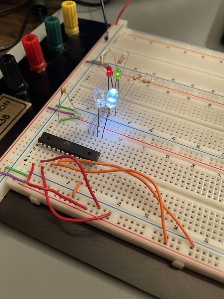
Anyway, WinCUPL also came with a simulator so I could create a bunch of sample input vectors to test and make sure it worked as expected in a variety of scenarios. I also eventually put it onto a breadboard for testing with some LEDs. I had a brief moment of panic when I thought the output enables for DSACK weren’t working correctly, but it turns out I was just being dumb and accidentally changing RW when I thought I was changing /AS.
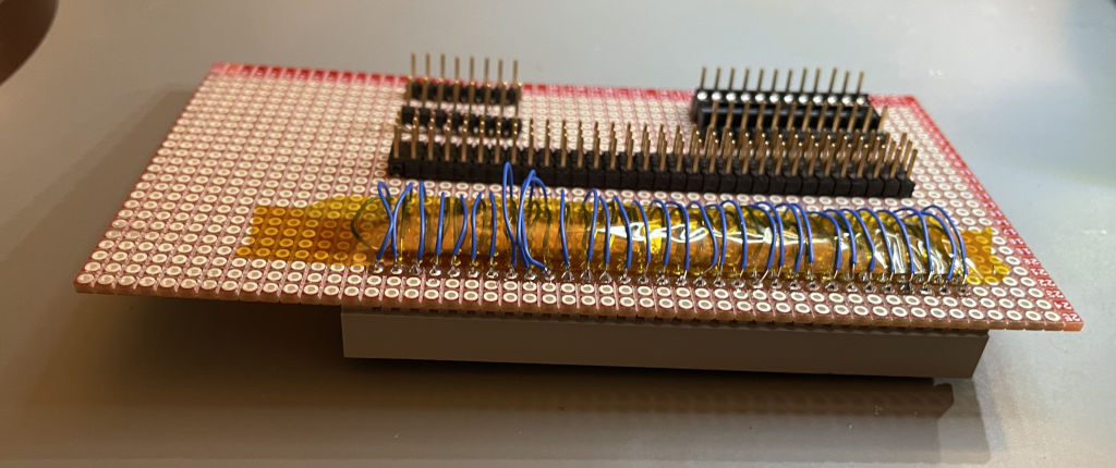
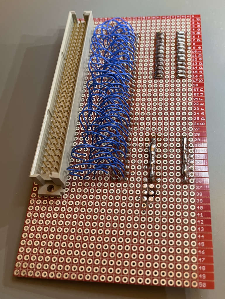
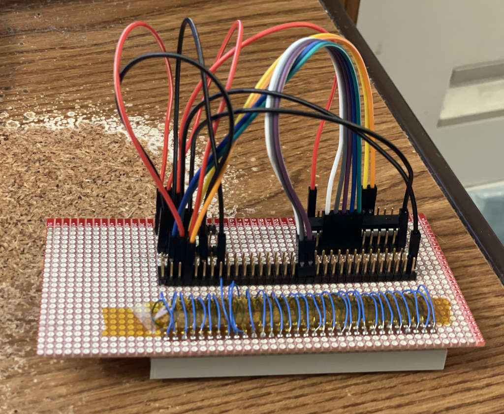
With my logic tested, it was time to throw together a PDS card. Ideally I should have designed a PCB, but by the time a PCB would have arrived, my free time around the holidays would have been over. So instead, I made the crazy decision to build it all on a protoboard. This required hours and hours of soldering. I wanted to design something that was reusable for possibly testing other concepts in the future, so I brought all 96 pins to a header. Soldering 96 tiny wires to 192 pins was…very tedious. Seriously, if you’re going to do this, just design a PCB instead. Don’t be like me.
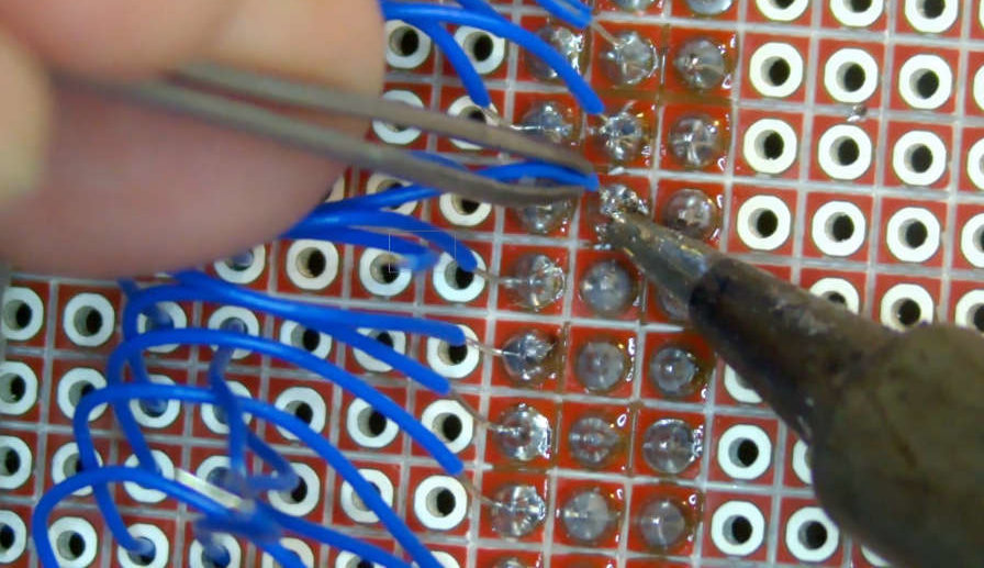
The end result is messy, but everything is connected! I got better at soldering the wires as time went on. I also added a socket for the ATF22V10C with headers for each pin, along with bigger headers for 5V and GND.
To start out, I decided to do some basic sanity testing to make sure that my PLD design worked properly. I tried to dump memory at 0xE0000000 in MacsBug with no PDS card installed in my LC 475.
DM E0000000
This results in a bus error:
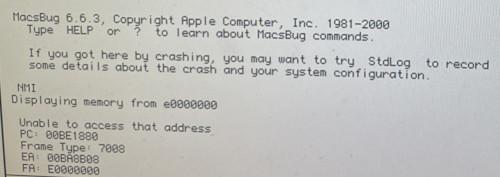
The bus error is caused by a timer. If enough time elapses after a read or write cycle has begun and nothing has responded to it, one of Apple’s chips will automatically assert /BERR to terminate the transaction. Otherwise the CPU would happily just wait forever.
Next, I hooked up the bare minimum needed for my PLD to make the CPU happy when it saw a read or write cycle: the address pins, /AS, R/W, and the /DSACK pins. And, of course, 5V and ground.
I inserted the card into my LC 475 and booted it up. The fact that it chimed and booted was a good sign. It meant I didn’t short any of the address lines, data lines, or bus control signals together. It also meant the machine was tolerant of my jumper wires. I retried the MacsBug test and it gave me different results this time:
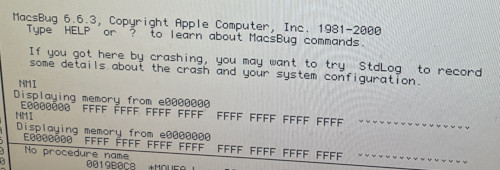
This is excellent! Instead of a bus error, it read back actual data. It’s all 0xFF, which probably makes sense. I’m not providing any data on the data lines yet. Maybe there are pullup resistors that provide a default value of 0xFF when nothing is controlling the bus. I’m not 100% sure. But regardless, there were no bus errors! My PLD made the CPU happy.
Here’s where things got really messy. If you think what I’ve done above is untidy, you ain’t seen nothing yet. I think this might be the jankiest LC PDS card ever created. If there was a Christmas ugly expansion card contest, I think I might win.
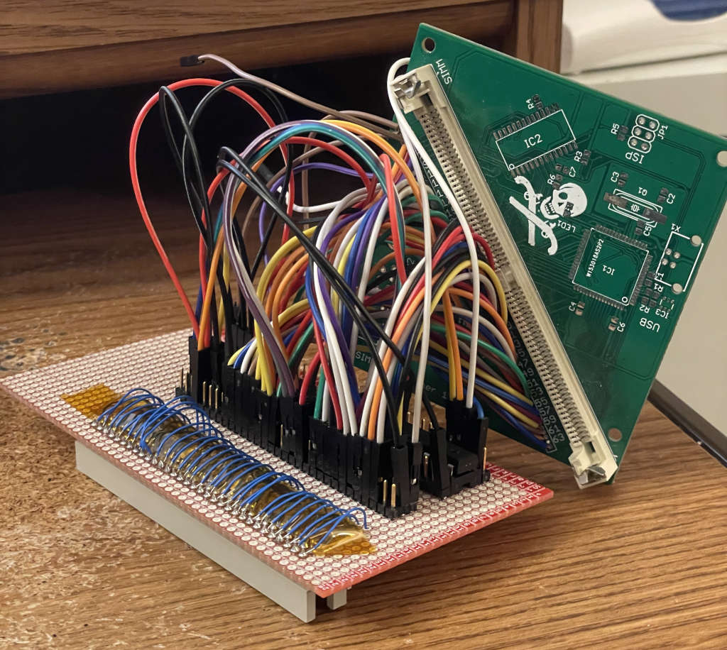
The green PCB is one of my Mac ROM SIMM programmer boards. It’s unpopulated except for the 64-pin ROM SIMM socket and a jumper wire soldered to almost every pin. If you pay close attention to my blog, you might remember it from my next-generation SIMM programmer prototyping. So essentially I just had to hook up almost all of these jumper wires to my PDS card. One by one.
That may sound easy, but it wasn’t. The jumper wires are too short, and it gets more and more difficult to squeeze them in place as you get closer to the end. Tweezers were very helpful for positioning things as I was finishing up. The final result ended up looking fairly chaotic, but hey, everything is connected!
Here it is, installed in my LC 475 in all its glory, with a corner of the programmer PCB resting on the 68LC040 CPU and my replica Lobos Board programmable ROM SIMM installed.
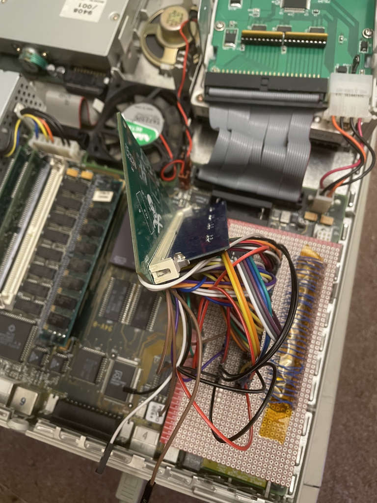
After my past adventures with accidentally damaging my LC 475 logic board’s onboard flash /WE pin by putting 12V on it, I was very careful to make sure 12V (VPP) was not shorted to any other pins in the circuit.
I cautiously powered on my LC 475. You may notice in the above picture I don’t have a battery installed, which means I have to flip the power switch off and on after the boot chime in order for the onboard video to work correctly.
It still booted just fine, so I didn’t screw anything up with all of my crazy jumper wires hanging around. Well, they might have been briefly broadcasting radio waves to my neighbors, but at least the computer worked. I couldn’t wait to try opening the Flasher utility and seeing if it would detect anything.
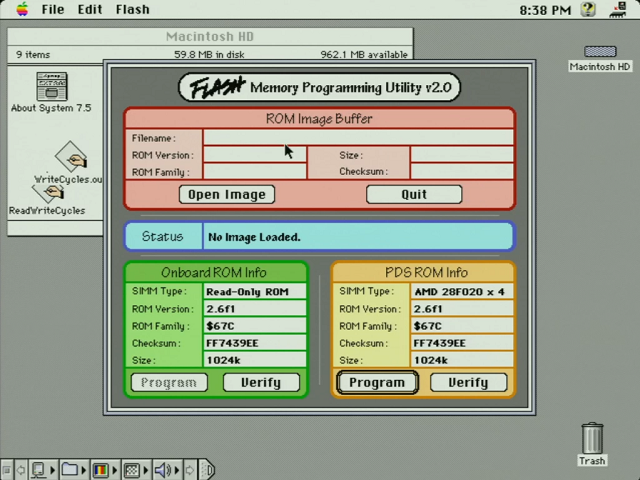
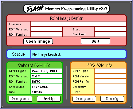
I’m always skeptical when something works on the first try, but it freaking worked. I had wired up every single one of those jumper wires correctly! The PDS ROM Info section showed a four-chip Am28F020 SIMM. This meant that both read and write cycles were working properly, because they’re both needed in order to perform the chip identification procedure.
This screenshot was taken after I had been playing with it for a while and had flashed the LC 475 stock ROM to the SIMM. Here’s a video of the programming process so you can compare it to how onboard ROM SIMM flashing worked.
When you program a ROM image through this PDS card, the UI updates as you do it. It tells you that it’s erasing, then programming, and finally verifying. Onboard SIMM programming didn’t allow this, because you can’t do Mac toolbox calls while you’re in the middle of programming your onboard ROM. There was no simple way to update the screen in that case. Also, it just leaves you back in the Flasher utility when it’s finished. It doesn’t automatically reboot like it does after reprogramming the same ROM you booted from.
I hope this trip down Apple developer memory lane is interesting to people out there. It has been a blast reviving this software and being able to share my findings with the world. I honestly could barely sleep last night after I got my PDS card working. I’ve never made anything like this before, and it’s opening up new avenues for me to learn more about hardware design. Is there any interest from people in actually owning one of these programmer cards? Obviously, it would be a polished PCB and not my rat’s nest depicted above. One concern is with so many different PDS slots out there, there would have to be different variants of the card. Either that or one mega card that has all of the required card connectors. That could get expensive though…
Either way, this definitely isn’t the end of this topic. I plan on hacking the Flasher software to also support modern ROM SIMMs in both the internal SIMM socket and the flash card. I’ll definitely share the process of figuring out how to hack the software. I’ve made some good progress on crudely hacking the code to prove the concept, but I want to make sure I do my final hackery the “right way” so that it’s maintainable going forward.


Thanks for sharing!
Every great electronics adventure usually involves a ridiculous rats nest. It’s been fun to follow along with yours. 🙂
Thanks ducksauz! I’m glad you enjoyed it! You are absolutely correct.
This is simply amazing work!
Thanks for sharing this.
Thank you Mr. Fahrenheit! I’m still recovering from the crazy soldering session, but it was totally worth it! (Not really, I probably should have either designed a PCB or only ran the wires I needed…)
WOW! What a journey!! Incredible work Doug!! I bet you’ve learned a ton on the way as well!! Your “big mess of wire” gives me great flashbacks to all the electronics labs we did when I was studying 😅😂!!
Should be fairly easy to also make a 040 PDS card using the same logic :). Let’s chat about that after the holidays.
Haha, thanks Joakim! It was quite an adventure. Yeah, I would like to see this turn into an 040 PDS card too. I think it will be a tad more complicated though because the 040 is faster. I’m guessing it’ll need some wait states. It’ll also require some research into the 68040 reference manual to see how different bus cycles are.
This is very very neat! Thank you for doing this. I love things like this. Wish I had a reason to use it, but fun to learn about nonetheless.
Ahh, somehow I missed your comment Matt. Thank you!
I’ve actually discovered that my PLD design seems to have a problem. When I use Intel chips, it seems to randomly fail during verification. The AMD chips seem to work okay though.
I need to revisit the logic in the PLD and make sure I’m handling the 680×0 bus totally correctly and meeting all timing requirements. One thing I’m suspicious about is that I’m not driving /DSACK0 and /DSACK1 high when I’m done with it — I’m just releasing it and letting the pullups bring it back up. It sounds like that’s actually bad and I’m not supposed to do it that way, so that’s definitely one thing to consider.
I have experimented a bit with building a Flash-Rom for the Power Macintosh. I was able to built a functional ROM module from a 7100 Rom-Dimm using AM29F800BB flash chips. I preprogrammed the chips before soldering them onto the module and had to tie the ‘RESET-pins of the AM29F800 to 5V. I connected the WE pins of the chips to a jumper to select either 5V or the WE-line on the Rom-Socket. I can boot the ROM from the socket without problems now.
I have not been able to reprogram the Rom in-system, though. The main problem seems to be the inability of the Flash-Utility v0.6 from the “PCI DDK A5” to work with current (final) Nitro/TNT boards. The software will always force a reboot with some corruption on screen before restart. The tool seems to set a register or something else in the GrandCentral ASIC that will not work on later boards and force a reboot without starting the flash-process. I would need a later version of the PPC-Flash utility to check this, though. The included system software will also not work with a final TNT/Nitro board unless some extensions are disabled (GC-realted).
Very cool project idea, Jonas! Unfortunately I’m not aware of any newer versions out there other than the TNT Flasher app. That was an advantage that I had working with these older machines — the Flasher app seemed newer than them.
That’s very interesting — I haven’t ever noticed a reset pin on flash chips before. That’s a new one for me.
I hope they didn’t do something to disable the in-system programming functionality in the final version of the GrandCentral ASIC!
Hey Doug,
I have just read the 2 posts since all of this started — quite quite mind blowing what you have discovered!, kudos to you to work on this and really looking forward for the program modification to support newer / current ROM ICs! :O
Hey Juan,
Thanks! It’s been fun learning how Apple did things back in the day. I still have big plans to modify the program — I just have to find time to do it! Too many projects, not enough time 🙂
Hey Juan,
Nice to read your story, I’m working on an GPIB controller
for the LC PDS so the tips on the address decode are nice.
I will make it with wire-wrap, should fit just fine inside the case and changes can be done fast.
Maybe that would also have been a good starting point for you, an wire-wrap 96 pin connector as you can put your jumper wire on to it.
Br,
Steve