A couple of weeks ago I found a really good deal on a Socket AM4 motherboard that supports the newest AMD Ryzen CPUs. The motherboard is an ASRock A520M/ac. It’s a very basic motherboard which doesn’t appear to be sold by any of the usual retailers anymore, but I couldn’t pass up on the deal, especially with the potential it had for being a fun learning project.
The reason I got such a good deal on it was because it was sold in non-working condition, but the seller and I both had a pretty good hunch about what was wrong. The seller said that they had bought it as an open box unit, but couldn’t get it to POST. However, they had only tried CPUs in it that were not compatible with the original BIOS version. I decided to have some fun and see if that was indeed the only problem. I didn’t have an older CPU available to easily test that theory. I did have a new Ryzen 7 5700G, which is only supported by BIOS revision P1.60 or newer.
Typically, there are several simple options for using a newer CPU with a motherboard that needs a BIOS update in order to support it:
- Borrow an older CPU just long enough to install an updated BIOS. AMD has a program for handling this if you don’t have an easier way to borrow one. I don’t know if this is a valid option if I’m not the original buyer of the motherboard. AMD’s documentation requirements in order to participate seem pretty stringent based on the linked instructions.
- Use the “USB BIOS Flashback” feature to update the motherboard’s BIOS even without a CPU installed. This particular motherboard doesn’t support that option.
- Send it back to the retailer or manufacturer to update it for you. I have no idea which retailers/manufacturers might do this. There’s no way that Amazon, for example, would provide this service.
It’s possible that ASRock would have tried to help me out if I had asked, but I decided to turn this into a fun personal challenge instead: upgrade the BIOS on my own without using an older CPU.
Visually and electrically inspecting the board
As soon as the motherboard arrived, I took several precautions before even thinking about powering it on with a brand new CPU installed. I checked out the components to make sure that nothing looked badly damaged. Everything looked fine, except for some white residue.
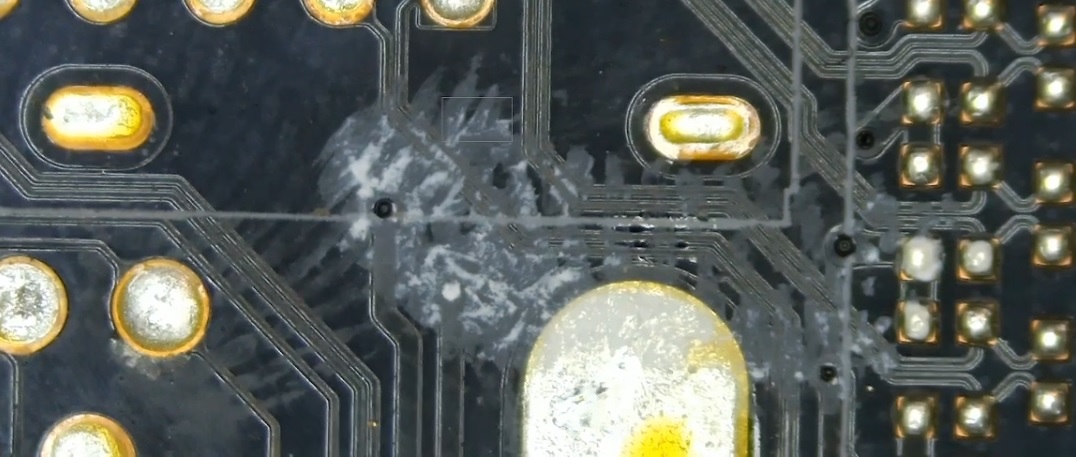
This kind of scared me at first. It looks like water damage based on some of the various repair videos I’ve watched on YouTube. But it was only localized to two small areas on the board, and it wiped right off with 99% isopropyl alcohol. I think it might have been thermal paste.
The other thing I did was check out the VRM. In one of my previous posts, I repaired my old motherboard that had failed in such a way that 12V was shorted to the CPU VCORE voltage, which fried the CPU. I wanted to make sure nothing crazy like that was happening on this board. After inspecting the MOSFETs with my multimeter, I was confident that this motherboard didn’t have any crazy short circuits between GND, 12V, and VCORE. This left me comfortable enough to continue on.
Reproducing the original problem
After I was confident that there weren’t any obvious catastrophic problems, I hooked up a power supply, put my Ryzen 5700G CPU in, connected a beep speaker, and powered on the motherboard by momentarily shorting the power button pins on the front panel header together. My thinking was at a minimum, I should hear it beeping as a complaint that I have no RAM installed.
Nothing happened, other than the CPU fan turning on. I didn’t have a heatsink on the CPU, but I plugged in a CPU fan to make sure the motherboard was satisfied. No worries – I was carefully monitoring the CPU temperature with my finger. It wasn’t even getting warm. No beeps, nothing.
I wasn’t super worried though. If the CPU isn’t supported by the current BIOS version, it’s very possible that it’s getting hung up earlier in the boot process than the RAM test. I powered everything off, removed the CPU from the motherboard, and focused on what it would take to update the BIOS.
Planning my approach
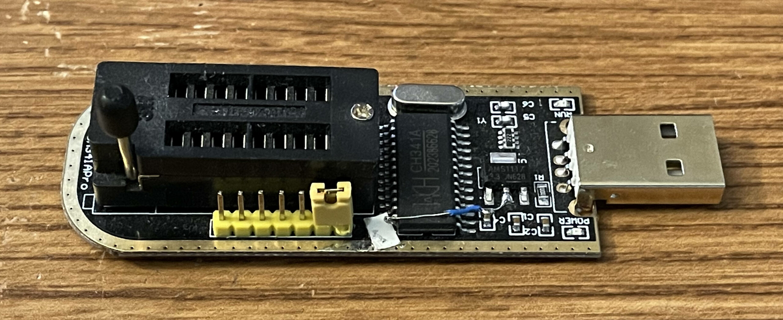
So here’s where the fun began. I needed to flash the new BIOS version onto the motherboard. I have a CH341A mini programmer that also came with a clip that can be used to hook up directly to 8-pin SOIC chips on circuit boards. You can find these all over Amazon and eBay for pretty cheap. I don’t want to link to them because the links will change over time, but you can search for CH341A programmer and find them. You do have to be careful with them, because at least some of them, including the one I got, have a major design flaw. They correctly power the SPI flash chip with 3.3V, but they provide 5V on the signal wires going to the chip. That would be bad, because typically 3.3V flash chips don’t want to see 5V on any of their pins, not to mention all of the other connected components on the motherboard. A lot of people have had success with these programmers even with the 5V issue, but I wouldn’t trust putting 5V on a pin that’s supposed to have a lower voltage. There is a simple hack you can perform on the board to fix this, which I already did a while ago. You can see my hack wire in the picture below.
Here’s a rough outline of what I decided to do:
- Find the chip and do research to verify that it’s safe to plug my programmer directly onto the motherboard through the SOIC clip, assuming the BIOS chip is a SOIC chip. I’ve also used hot air to remove a BIOS chip for programming in the past, but I wanted to avoid doing that if I didn’t need to.
- Dump the existing chip contents, just in case I screw something up.
- Compare the existing chip contents to a newer BIOS update downloadable from ASRock.
- Assuming the existing chip contents and the update file look to be in the same style, try flashing the update file directly to the chip.
- Put the CPU back in and try again.
Finding the BIOS chip
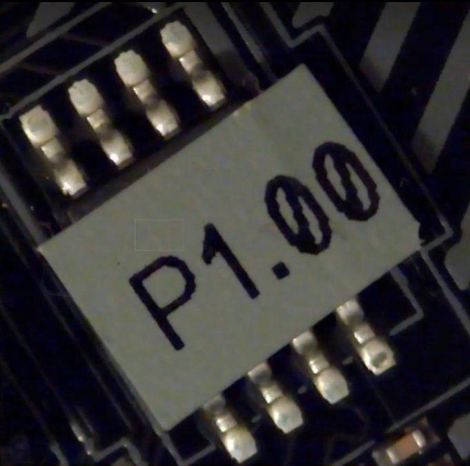
It wasn’t very difficult to find the chip. On most modern motherboards I’ve seen, the BIOS chip is an 8-pin SOIC chip that’s pretty hard to miss. Usually it’s not in a super crowded area of the board. They can be easily mistaken for voltage regulators, so definitely check your part number to make sure it’s a flash chip! In my case, it was super easy, because there was a big sticker on it that indicated the original shipping version of the BIOS: P1.00.
I won’t go so far as to say this was promising, but it was at least evidence that this particular board did not originally ship with a new enough BIOS revision to support my 5700G out of the box. My theory was still plausible.
Identifying the BIOS chip in depth
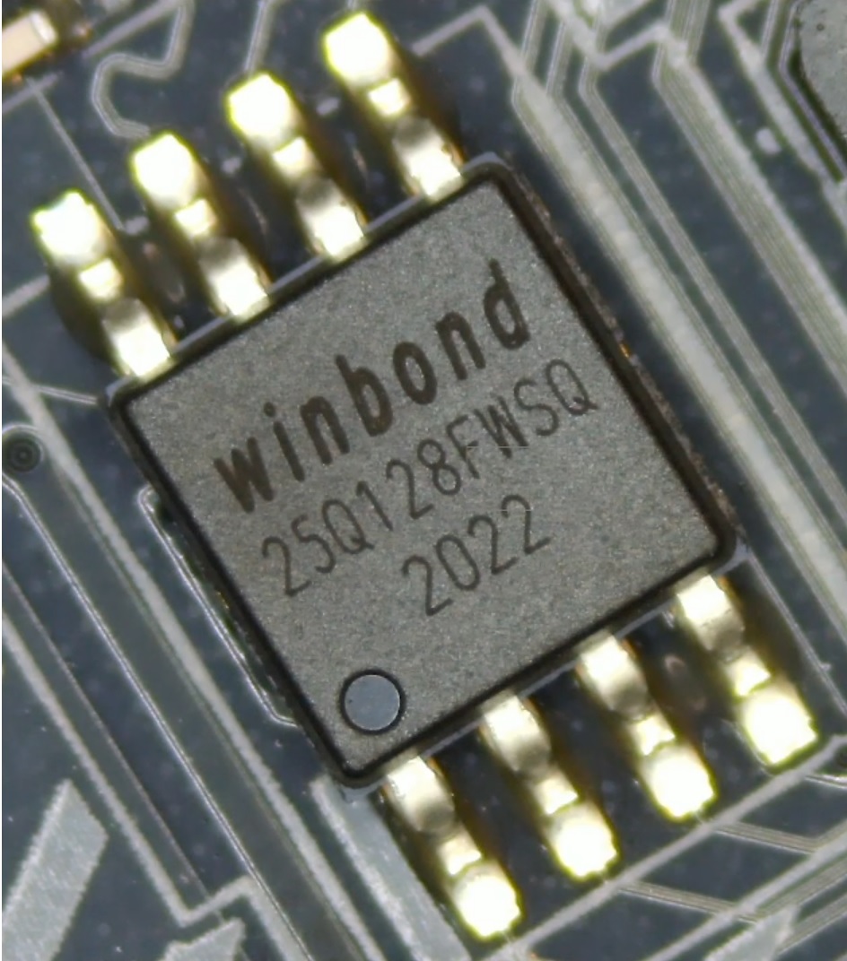
As soon as I peeled the sticker off, I was greeted with the actual part number of the BIOS chip. It’s a Winbond chip, with the marking 25Q128FWSQ. With some quick Googling, I easily found the datasheet directly on Winbond’s website. Checking the table on page 96 of the document, I was able to determine that the actual part number for this chip is: W25Q128FWSIQ. There’s a table on page 95 that breaks down the part number:
- The first W means Winbond. Never would have guessed that!
- The 25Q means it’s an SPI flash with 4 KB sectors and dual/quad I/O. Dual/quad I/O means that it can optionally use two or four of the chip’s pins as parallel data I/O pins, rather than normal SPI, which has one input pin and one output pin.
- The 128F means the size is 128 megabits (16 megabytes).
- The next W means that the supply voltage is 1.65 to 1.95 volts. In other words, it’s a 1.8V chip with a little bit of wiggle room. This was originally shocking to me because I’ve typically worked with 3.3V BIOS chips, but it appears that AMD motherboards have been using 1.8V flash chips for quite some time now.
- The S means it’s an 8-pin SOIC chip. You can buy this chip in other forms that are much less convenient to work with as well, such as 24-ball BGA.
- The I means it has an industrial operating temperature range, which they declare to be -40 to 85 degrees Celsius (that’s -40 to 185 degrees Fahrenheit, for those of us in the United States, Bahamas, Cayman Islands, Liberia, Palau, Federated States of Micronesia, and Marshall Islands).
- The Q is a special option that means “QE=1 in Status Register-2”. More on this later!
Figuring out how to program a 1.8V chip
The 1.8V supply voltage on the BIOS chip caught me a little off guard. I was originally expecting to be ready to go for flashing a 3.3V chip with my CH341A mini programmer and SOIC clip. Now that idea was out the window. Everything I said above about 3.3V was wrong. What I really needed was for the chip to be powered by 1.8V, and the signals going in and out of the chip to be 0-1.8V. It turns out I wasn’t the only one to run into this dilemma. A lot of the CH341A kits on the market include a 1.8V adapter board. I bought one, and impatiently waited for it to arrive.
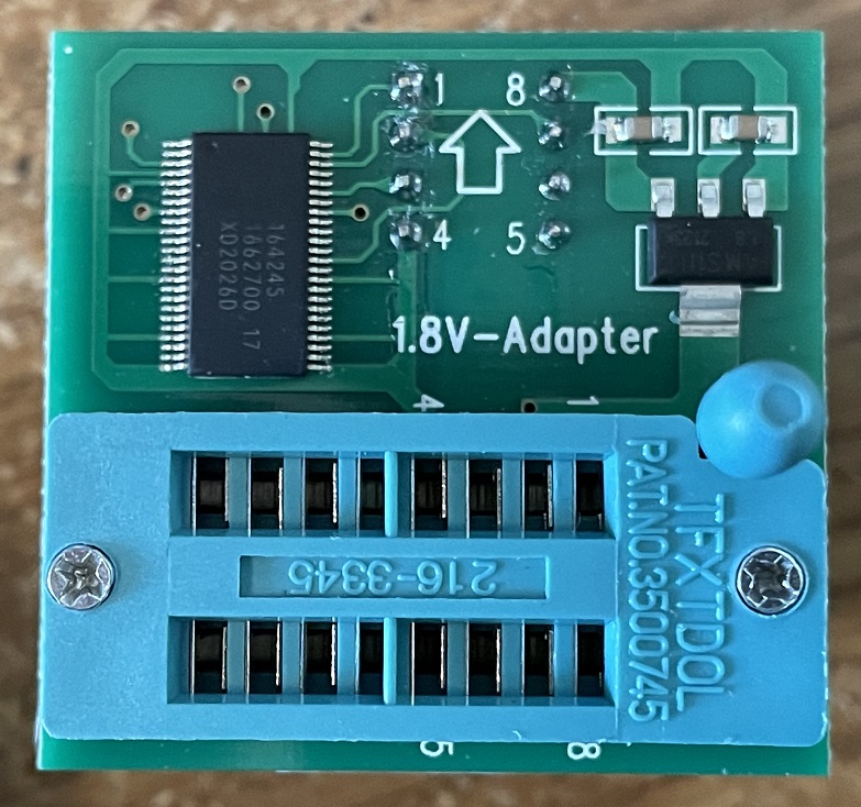
It plugs inline between the CH341A programmer and the SOIC clip to drop the voltage levels down from 3.3V to 1.8V. The 8 pins near the top around the arrow on the silkscreen actually stick out of the underside of the board. You are supposed to plug those into the ZIF socket on the CH341A board. The ZIF socket on the 1.8V adapter board (the blue piece in the bottom half of the picture) provides a 1.8V equivalent version of the ZIF socket on the CH341A programmer. I saw some reviews and comments saying that the 1.8V adapters have problems and don’t work, so with the help of my handy dandy multimeter, I reverse engineered the one I received to convince myself that it would do what it was supposed to do. Here’s a little schematic I made in KiCad showing the circuit (click to view full size in a new tab):
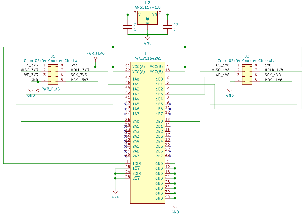
The board is actually really simple. It consists of an AMS1117 linear regulator to create a 1.8V power rail from 3.3V, a few capacitors (I’m curious if an electrolytic cap should be on there too), and a Nexperia 74ALVC164245 translating transceiver. This transceiver has two ports of eight voltage level shifters which translate voltages between VCCA (3.3V on this board) and VCCB (1.8V on this board). Each port has two configuration pins shared by all 8 of its shifters: enabled and direction. On this board, port 1 is used for translation from 3.3V to 1.8V, and port 2 is used for translation back from 1.8V to 3.3V. In particular: the CS, MOSI, SCK, WP, and HOLD pins are 3.3V->1.8V and the MISO pin is 1.8V->3.3V. This makes sense with how most SPI flash communication works, at least in normal SPI mode.
The AMS1117 is commonly cloned by all kinds of manufacturers, so I would be surprised if the part on my board was a genuine part by Advanced Monolithic Systems. The 74ALVC164245 is made by several different manufacturers including Nexperia, Renesas, and TI (links are to datasheets). One thing to carefully note is that only Nexperia’s datasheet specifies that it’s actually capable of being used as a 3.3V<->1.8V level translator. The Renesas datasheet says that VCCB is only capable of being 5V, and the TI datasheet doesn’t talk about VCCA/B any less than 2.5V. Honestly, all of these datasheets are kind of weird about the supported voltages, but the Nexperia one specifically says that VCCA/B can both go down to 1.5V. A message on NXP’s forums prior to the Nexperia spinoff confirms that it will work for 1.8V translation.
I plugged it into my CH341A board and tested it with my multimeter in voltage measurement mode to make sure the regulator was spitting out 1.8V and the output signals were all 0 to 1.8V. It appeared to be working just fine.
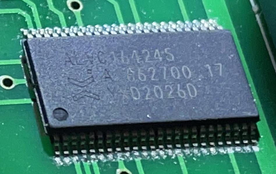
Quick side note: The chip on my board is marked as a Nexperia part, although in the photo above you can’t see the manufacturer marking because it shows up in the darker upper half of the chip. The marking on this chip is pretty weird because half of it only shows up in certain lighting conditions. I don’t know whether that’s a good or a bad sign in terms of potential counterfeiting, but the chip seemed to behave fine for me! Here’s a better view where you can see the etched portion with the Nexperia logo.
Determining if I can clip directly onto the chip
With the 1.8V challenge out of the way, I started thinking about whether the motherboard would be okay with me clipping directly onto the flash chip and programming it. This is where it can get a little tricky, because every motherboard is different. The one thing I wanted to figure out was: what other chips are connected to the same power rail that powers the SPI flash chip? Where else does the 1.8V go? The reason this is important to understand is because if too many things are powered by that 1.8V rail, then they will all try to be powered by the programmer. And the programmer may not be able to supply enough power. Additionally, any other chips powered by the same rail might interfere with the communication between the programmer and the chip.
I put my multimeter into continuity mode and looked for anything else hooked up to pin 8 (VCC) of the chip. I only found it going to a couple of transistors nearby. It’s impossible to test everything for sure because some parts are BGA, so you can’t know for sure if a particular ball under the chip is on the same voltage rail. However, there will be capacitors nearby any chip, and some of those capacitors would be connected to the same voltage rail if it was powering the chip. I didn’t see anything like that. Having schematics for the board would sure have been nice.
I also measured the resistance of the rail and it wasn’t super low, which is another good sign. I honestly don’t remember the exact numbers, but I just remember it wasn’t down in the tens of ohms.
Verifying pinout
I also wanted to verify that the CH341A’s pinout matched the pinout of the Winbond flash chip. I had no doubt that it did, but it’s still a good idea just to double check. SPI flash chips all follow the same JEDEC pinout, so it would be really strange for a chip not to match. I’m really glad I double checked though, because it caused me to think about the WP and HOLD pins a bit (pins 3 and 7). The CH341A mini programmer hardwires those two pins to 3.3V, meaning that the chip is not write protected and not being paused. This is easy to see by looking at the traces on the bottom of the programmer circuit board. Pins 3, 7, and 8 are all wired directly to 3.3V.
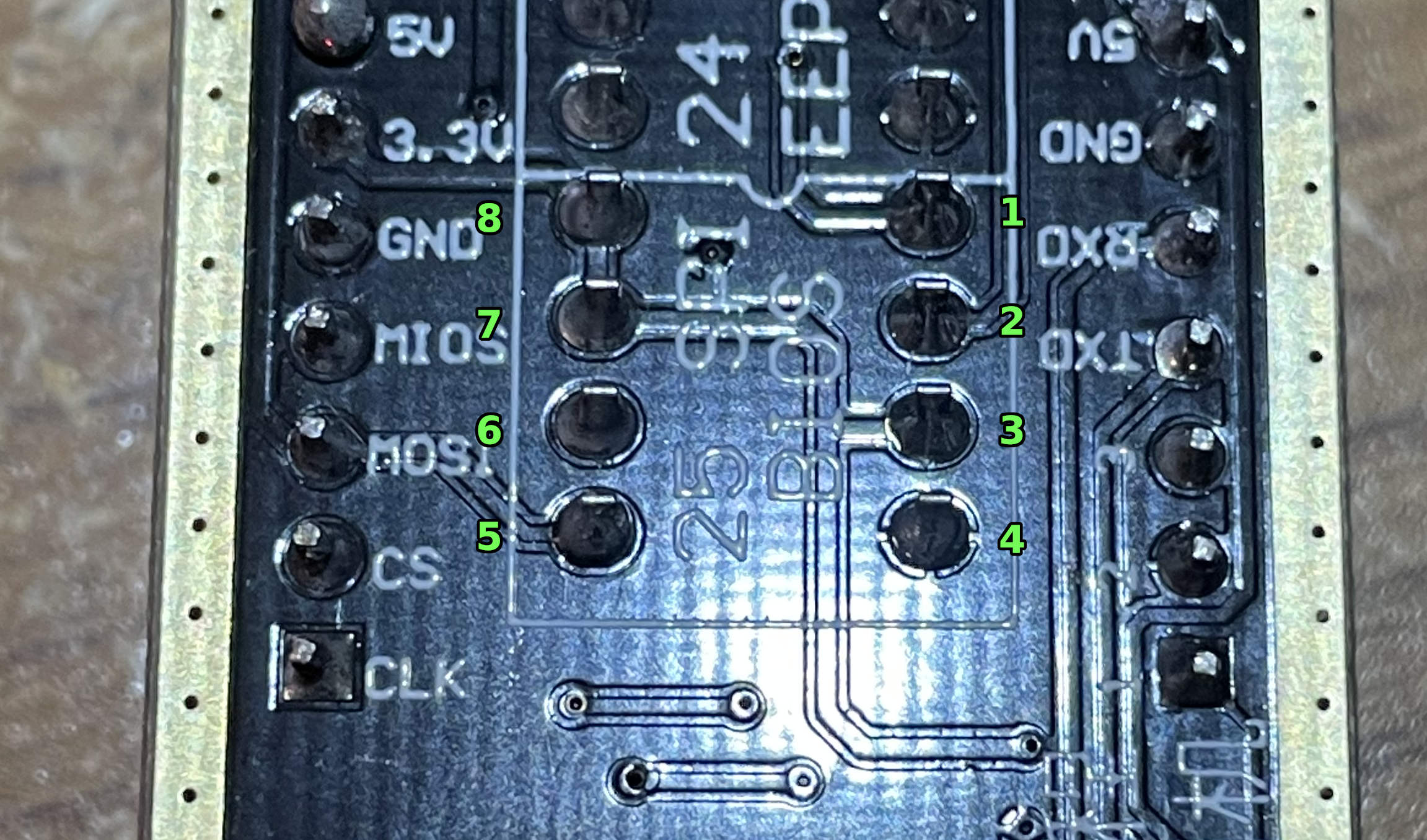
We are using the 1.8V adapter, which means they’re effectively hardwired to 1.8V through the level shifter chip instead.
On this flash chip, the WP and HOLD pins optionally end up being treated as IO2 and IO3 pins when you’re in quad SPI mode. I remembered what I noted about the part number indicating that QE=1 in status register 2. When I read about status register 2 on page 19 of the Winbond datasheet, I found that the QE bit essentially decides whether the pins are IO2/IO3 or WP/HOLD. Because this chip defaults to QE=1, the pins default to IO2/IO3 instead of WP/HOLD. Then, I found this interesting note at the bottom of the page:
WARNING: If the /WP or /HOLD pins are tied directly to the power supply or ground during standard SPI or Dual SPI operation, the QE bit should never be set to a 1.
I began to realize that this could be a problem with the way the CH341A programmer is set up. The WP and HOLD pins are effectively tied directly to the power supply, and the QE bit defaults to 1. Sure, it’s through that voltage level translator chip on the 1.8V adapter board, but if the datasheet is saying not to tie those lines to VCC or GND with QE=1, it likely means that IO2 and IO3 could potentially be driven by the chip even during standard SPI operation when QE=1.
The QE bit is non-volatile, meaning it remembers its value across power cycles. There’s a chance that it’s already been turned off by ASRock, and this could be a complete non-issue. I didn’t want to chance it though, so I added 1kΩ series resistors on pins 3 (WP) and 7 (HOLD) of the cabling for my SOIC clip. This effectively made it so WP and HOLD were pulled up to VCC through a 1kΩ resistor rather than hardwired to VCC, thus avoiding any conflicts. Some people end up modifying the programmer board itself to do this, which makes a lot of sense, especially if you are putting a DIP style BIOS chip directly onto the programmer. That wouldn’t work in my case because the 1.8V adapter board would also need to be modified.
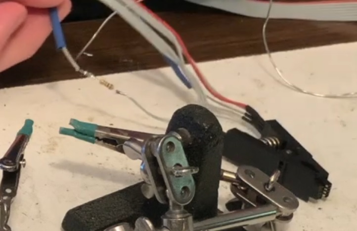
In the picture above, you can see a newly-soldered resistor on pin 7 of the clip along with the tube of heatshrink that is about to be pulled over the resistor and applied with heat to protect it.
With this mod in place, this chip clip should mostly be fine to use in the future on any motherboard. The exception would be if the board itself has pulldown resistors on those lines. If that happened, the pullup and pulldown resistors would effectively create a voltage divider circuit, which would potentially result in a weird voltage halfway between 0 and 1.8V on those two pins. So in the future, if this clip doesn’t work on a particular motherboard, I might need to switch to an unmodified clip instead.
Reading the existing BIOS from the chip
Finally, after all of that prep work, I was actually able to try something out. I installed flashrom on my Linux computer. It is a utility for reading/writing data to/from flash chips. It’s even capable of flashing the BIOS chip live on the computer it’s running on, in many cases. It includes support for several USB programmers including the CH341A. I grabbed the latest sources from the Git repo and built them myself with “make”, but it probably would have worked fine if I installed it through a package manager instead. I just wanted to make sure I had all of the latest fixes.
I plugged my 1.8V adapter into my CH341A programmer, then plugged the modified SOIC clip into the 1.8V adapter. Here’s a view of the complete stack and the chip clip:
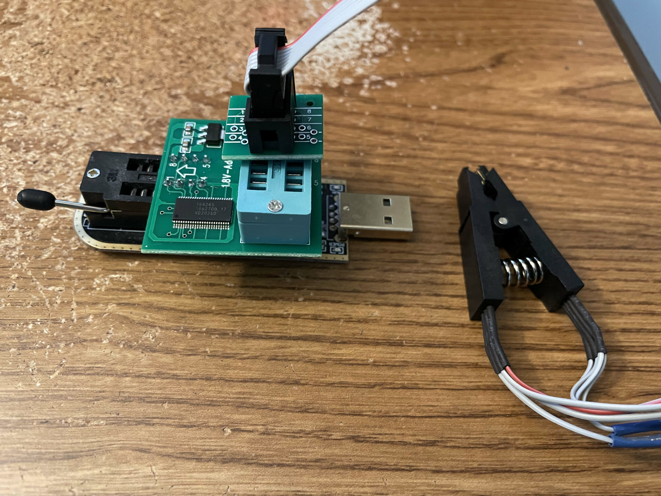
With the motherboard completely disconnected from everything else, no CPU installed and no RAM installed, I carefully clipped the SOIC clip onto the motherboard, ensuring it was aligned perfectly. Unfortunately, this is the only image I took of the setup and it was a pretty low resolution.
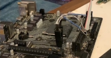
Next, I plugged the programmer into my Linux computer’s USB port very slowly, ready to yank it out immediately at the first sign of any magic smoke escaping. But everything seemed fine, nothing got hot, and I was ready to go.
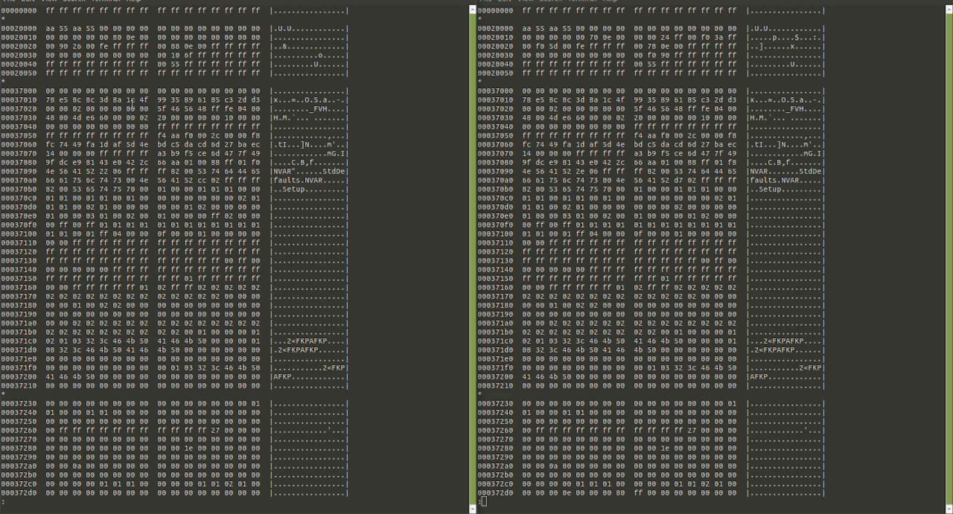
$ ./flashrom -p ch341a_spi
flashrom v1.2-552-gea0ae15 on Linux 5.11.0-40-generic (x86_64)
flashrom is free software, get the source code at https://flashrom.org

Using clock_gettime for delay loops (clk_id: 1, resolution: 1ns).
Found Winbond flash chip "W25Q128.W" (16384 kB, SPI) on ch341a_spi.
No operations were specified.
After I saw this output, I knew I was in business. flashrom was able to communicate with the chip and identify it. I was relieved that I didn’t need to bother desoldering it from the motherboard. So I read the chip:
$ ./flashrom -p ch341a_spi -r readback.bin
flashrom v1.2-552-gea0ae15 on Linux 5.11.0-40-generic (x86_64)
flashrom is free software, get the source code at https://flashrom.org

Using clock_gettime for delay loops (clk_id: 1, resolution: 1ns).
Found Winbond flash chip "W25Q128.W" (16384 kB, SPI) on ch341a_spi.
Reading flash...
After a little over 2 minutes, it finished.
Reading flash... done.
I did another readback and diffed the two readbacks to make sure everything was reading back consistently, and the two readbacks were identical.
Comparing the existing BIOS to a new BIOS
I decided to download BIOS version 1.80. My thinking was that I could update to the newest version as of this writing (1.90) directly through the running system as a final test. The first big clue was that the update file (A52MIX_1.80) was exactly 16 MB. That’s perfect, because it will fill the entire chip. Comparing it to the dump, it was obvious that the file was structured in exactly the same way as the current chip contents.
This was enough for me to give it a go. What’s the worst that could happen? On a lot of motherboards, there is other information stored in the BIOS flash chip, and the BIOS update process is smart enough to leave that section of the chip alone. For example, when I manually flashed a Dell computer’s BIOS chip, I had to re-enter the service tag info. I’ve heard that depending on the motherboard, it may also contain other info such as the Ethernet MAC address, serial numbers, etc. This is why it’s important to dump the original flash first. With the original dump intact, it may be possible to locate where the special configuration info is located and reinsert it back into the chip, especially if you can diff the dump against the BIOS update file for the same version. I just decided to go for it, knowing that I could always reflash the chip again later.
Writing the new BIOS to the chip
Programming the new BIOS to the flash chip was a breeze with flashrom:
$ ./flashrom -p ch341a_spi -w A52MIX_1.80
flashrom v1.2-552-gea0ae15 on Linux 5.11.0-40-generic (x86_64)
flashrom is free software, get the source code at https://flashrom.org

Using clock_gettime for delay loops (clk_id: 1, resolution: 1ns).
Found Winbond flash chip "W25Q128.W" (16384 kB, SPI) on ch341a_spi.
Reading old flash chip contents... done.
Erasing and writing flash chip... Erase/write done.
Verifying flash... VERIFIED.
The whole process took about 10 minutes.
Testing the new BIOS
After all of this work, I was ready to go. I unplugged the programmer, removed the clip from the chip, put the CPU back in, again with a “fake” CPU fan, plugged in the power supply, and powered it back on.
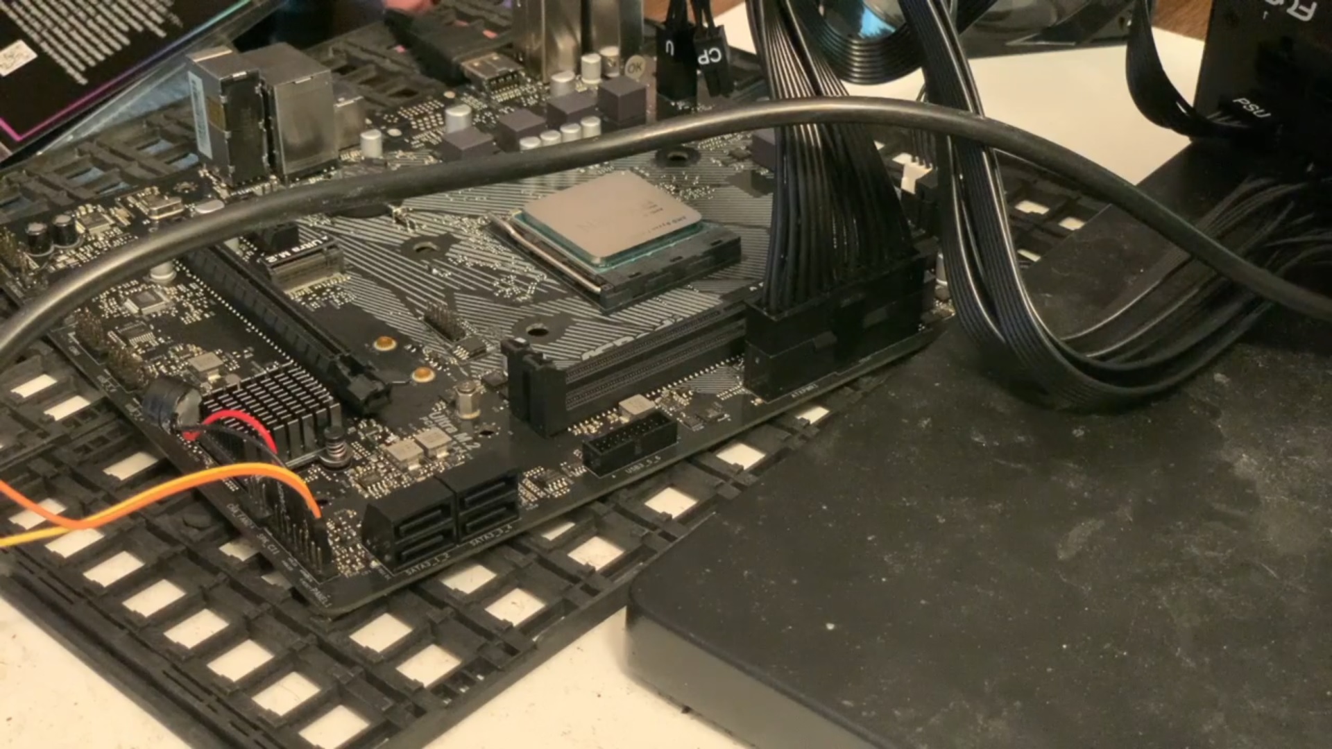
Again, I monitored the CPU temperature very closely with my finger. I didn’t want to overheat it. The speaker began beeping immediately. This is where I started to get pretty excited. I had made progress! I was getting RAM error beeps, whereas before, I was getting nothing. The board was showing signs of life! So I shut it off, installed RAM, and tried again.
This is where I kind of freaked out. I powered it back on with the RAM installed. No immediate beeping occurred this time, which was good. I held my finger on the CPU and it wasn’t getting warm. After about 30 seconds it did start warming up. After 40 seconds, I got a little paranoid about the temperature and turned off the power supply just to be safe. Just as I flicked the switch on the power supply, the boot screen showed up on the video output!

Success! I cleaned off the CPU with alcohol because I had been touching it, and fully installed the heatsink/fan. Then, I powered it back on. It booted right up and I went into the UEFI setup.
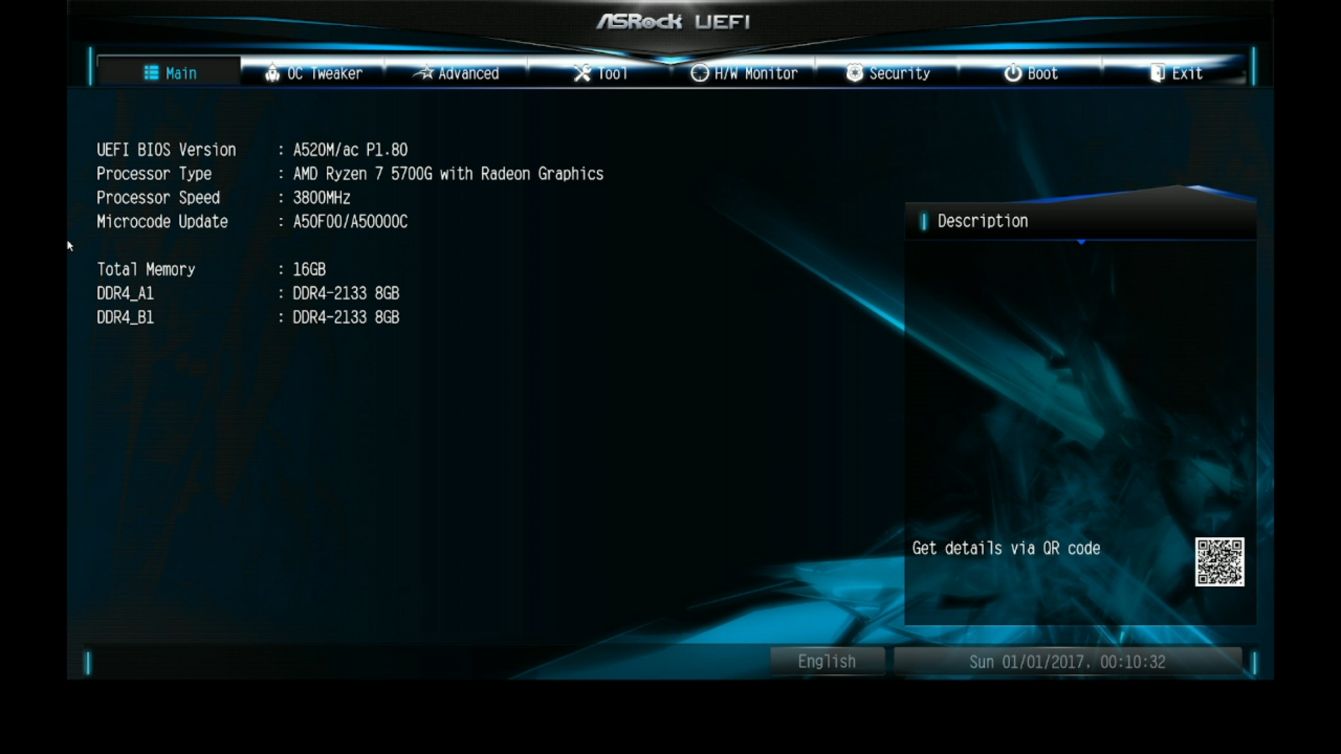
Finally, I installed the latest 1.90 BIOS version from a flash drive through the standard “Instant Flash” BIOS update capability, and it also worked fine. I checked, and I still have a valid ASRock Ethernet MAC address, so I don’t think I lost any important factory values. It all seems to work fine. One thing I could do is re-dump the chip and compare it against the matching BIOS update file. That might reveal sections of the original dump that contain any additional data. In my case, I’m pretty sure this motherboard doesn’t store anything important in the SPI flash chip other than the BIOS itself. It might also store some nonessential settings that are safe to lose.
Conclusion
I was able to successfully “fix” this motherboard without access to an older CPU! This strategy won’t always work on every board, but it worked on this one. Some boards might not allow you to flash the BIOS chip in-circuit. Other boards might store important config info such as the Ethernet MAC address in the chip, which will complicate matters.
The cool thing is I was able to do this with a few simple tools widely available for purchase online combined with an excellent open-source utility. I will say that it’s really frustrating that the tools have design issues that require you to hack them up before you can safely use them for their intended purposes. The CH341A programmer needed a hack in order to supply 3.3V properly on all of the pins, and the SOIC clip needed a hack in order to more safely control the WP and HOLD pins — a hack that would probably be better to put on the programmer and 1.8V adapter boards rather than the clip. Most people aren’t equipped to do these hacks, so it kind of defeats the purpose in a lot of cases. I can’t argue with the very reasonable price on these programmer kits, but it would be nice if they were sold with correct/safer designs in the first place.
Fancier motherboards that can be updated without a CPU installed are pretty cool. That’s a great feature that the manufacturers dreamed up, but not every board supports it. It costs pennies to ensure the BIOS chip is wired up on the motherboard in a way that it can be reprogrammed in-circuit, and it would be easy for the motherboard manufacturers to let us know what sections of the BIOS chip need to be preserved across updates. In a future world where the popular cheap SPI flash programmers don’t have any crazy design issues, it would be nice to see all of the motherboard manufacturers embrace them. Why can’t we button up the process I followed in this post and make it easy for everyone to do? It would save people a lot of headaches in situations like this. Imagine a world where someone with this same problem can buy a simple off-the-shelf BIOS reprogrammer that is already wired properly, clip it on, download the latest update file from the manufacturer’s site, and flash it directly to the board.
The last thing I want to say is that lots of people have done the exact thing I did in this post. There’s nothing really novel about what I did, but I thought it would be interesting to describe the whole process from start to finish, including the roadblocks I ran into. Right now, it’s more complicated than it should be, and most of that complication is just due to easily solvable design issues with the current generation of widely available programmer hardware.


Woah, that’s some serious care going into the “ugh it’s 1.8V” problem. When I recovered my previous board (X370) I just used a 5V-3.3V shifter module – plugging 3.3V into the “5V” side resulted in 2.8V on the “3.3V’ side which was “a bit better”™ so I used that. Surprise, the flash didn’t care. Seems like these chips are unofficially 3V tolerant and you can just YOLO it with a direct 3.3V connection.
Also my board had a 2.0mm pitch SPI header and I didn’t have connectors for that back then (nor did I have a chip clip). I, uh, managed to fit some 2.54mm connectors on the pins – couldn’t connect *all* pins but it still worked (at a low speed) without GND.
The ethernet MAC addresses are more likely to found in the individual NIC’s controllers. In any case, the sole use of them is to guarantee uniqueness in a collision domain, so picking one at a random is entirely reasonable.
@greg: Haha, I’m glad the YOLO worked out for you! I’m paranoid because those SPI pins could also potentially go elsewhere on the board onto other components. Probably mainly just the CPU which I removed anyway, but still…it scared me enough. This board also has some kind of SPI header next to the BIOS chip. It would sure be nice if that header was standardized.
@dsr: I agree for the most part, but it sounds like certain boards do store the MAC address in the BIOS. It probably depends on the Ethernet chipset. You’re right that you could just pick a random one, if you could figure out where to put it in the flash chip. Either way, it didn’t matter on this board, but that’s one of the reasons I kept a dump of the original BIOS just in case I later discovered that I trashed something important.
@greg: Makes sense, flash controllers use a charge pump to get up to 5V for reading, 10V for programming, 20V for erasing. There’s a bit of leeway in the spec and a bit of loss and ripple filtering that happens in the charge pump. If you’re over voltage on the input, it might reduce the life a little but not enough to matter.
I just double-checked. If I make a 5-stage MOSFET charge pump in Falstad simulator, a 5 V input/clock has an output of 24 V, while a 3 V input/clock creates a 20 V output—not 14.4 V as you’d expect from a linear component.
You could trace the pins from the header and see if they match the ones from the SPI chip with a multimeter (continuity test). With some of the hooks like here: https://sigrok.org/wiki/Probe_comparison you can then connect to the header or the chip itself. There are also some more expensive programmers around which allow you to adjust the voltage from 1.8-5V.
[…] Upgrading a motherboard’s BIOS/UEFI (the hard way) […]
@plusminus: The motherboard manual actually documents the header pinout (it’s for a TPM module), and I verified the connections with my multimeter. Even though it’s a TPM header, the BIOS chip select is also present. The big challenge I ran into was it was a smaller header so I wasn’t sure if I could fit my jumper wires onto it. What I would really like to see is for all motherboard manufacturers to standardize on a BIOS programming header…probably wishful thinking though.
I’ve also heard of people swapping the flash chip on a live system (when they were in sockets) to recover a flash chip that needed programming. You boot with the good flash chip, swap it out for the bad flash chip, and then run the regular “upgrade my flash” binary to write good data to the flash chip. Probably only works if you have two identical motherboards 🙂
can I use a windbond 25q128fvsq (fv)=3.3v bios chip
a 3.3v chip use it on a motherboard that has a 1.8v bios chip
or will the 3.3v chip not power on when installed on the motherboard
im asking because im repairing a asus b450i and it has a
gigadevice(25LB128CSIG)(1.8v) bios chip and I was wondering if I can use
the 3.3v bios chip on there
Hi jj, I wouldn’t expect it to work. If you look at the datasheet it’s not rated to operate at that low of a voltage. I would recommend finding a true 1.8V chip instead.
How do you think this would work on a eight pin bios chip for a hard drive PCB. The thing to do here the most accounts is to swap the chip and the chips been around for a while certain it still has information on it but one of the pens wiggling around like a Michael Phelps next Olympics who knows what it’s gonna do if it’ll even make it, another one is snapped off the interior part of it still intact I can see it I sold it, but the whole board to match with the chip seems to me should be possible for me to write to that chip that should be an easy solution trying to mess with taking the good shape off rig up an old chip so I can read it and then get it in to be attached to the new board. Problem is I don’t know if that’s possible in this case I don’t know if this bios come out like yours and that we’re working with very different things. Online seems to say no but heck they haven’t tried. Plus this swaps been going on for decades technologies changed a good deal in the last five years. I have essentially set up you got another little thing that’s sore pin chips right off the board. Not the claps with teeth but a sort of wand, supposed to be more precise and quicker but I have that whole set up ready for situation just like this. Question as I said about making these Microsoft on these pens to have it sent on the board or do I just need to give me a Nuff of a connection to read what’s on it, and not bother with the southern chip that’s already on there. That seems like the easy solution all the way around, if that were possible seems to be doing that rather than worry about learning to solder shipping or drive off it’s not like this is New technology
Hi Marty, it’s hard to know for sure what’s possible without a part number. I think desoldering the chip and reading it out of circuit is probably the best bet for something like that, but desoldering a chip from an important PCB probably isn’t the best way to learn either.